Part 2c: disabling external 3K expansions
Posted: Fri Nov 19, 2010 5:51 pm
The original signals /RAM1, /RAM2 and /RAM3 on the mainboard are not anymore connected to and driven by UC4. On the one hand they are used by UD9 to separate the CPU and VIC data bus as necessary. Those inputs are now open, fortunately for the test in the preceding posting this doesn't matter, as floating TTL inputs are regarded as having high level by the respective gate - thus having no bad influence on the operation of UD9 in this case.
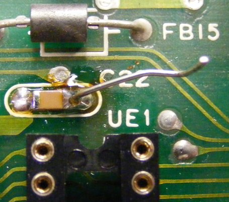
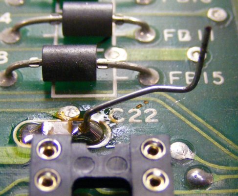
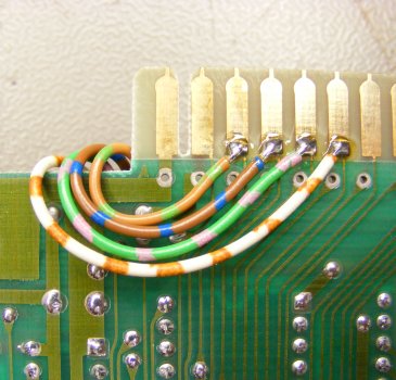
But on the other hand there might be other input gates for the RAM select lines on the other side of the expansion port. The open TTL inputs of UD9 place a signal level of ~2.4 volts on the RAM select lines, which is undefined for CMOS inputs! For that reason, it is necessary to put a well defined high level on the original /RAM1 to /RAM3 signal lines. This is done with three 4K7 SMD resistors connected to the original RAM select lines against the +5 V supply voltage, on the solder side, as shown below:
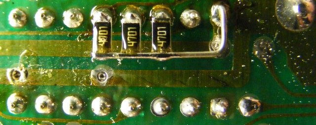
You see the soldering side of UC4, and the expansion port faces to the right. The three resistors are soldered against pins 12, 13 and 14 of the socket, and the +5 V supply voltage is taken from pin 16 of the socket and connected via a solid wire to the other side of the resistors. The assembly actually "floats" roughly 1/2 mm over the mainboard.
Here's a small test program to check whether the RAM in the range $0600 to $1DFF is functional:
This completes part 2 of the mod. It is now possible for the VIC chip to access the entire range of $0000 to $1FFF.
Part 3 will follow tomorrow.
Cheers,
Michael
But on the other hand there might be other input gates for the RAM select lines on the other side of the expansion port. The open TTL inputs of UD9 place a signal level of ~2.4 volts on the RAM select lines, which is undefined for CMOS inputs! For that reason, it is necessary to put a well defined high level on the original /RAM1 to /RAM3 signal lines. This is done with three 4K7 SMD resistors connected to the original RAM select lines against the +5 V supply voltage, on the solder side, as shown below:
You see the soldering side of UC4, and the expansion port faces to the right. The three resistors are soldered against pins 12, 13 and 14 of the socket, and the +5 V supply voltage is taken from pin 16 of the socket and connected via a solid wire to the other side of the resistors. The assembly actually "floats" roughly 1/2 mm over the mainboard.
Here's a small test program to check whether the RAM in the range $0600 to $1DFF is functional:
Code: Select all
1 POKE55,0:POKE56,6:CLR
2 X=RND(-2):FORT=1536TO7679:POKET,RND(1)*256:NEXT
3 X=RND(-2)
4 FORT=1536TO7679
5 IFPEEK(T)<>INT(RND(1)*256)THENPRINT"ERROR IN";T:STOP
6 NEXT
7 PRINT"ALL OK!"Part 3 will follow tomorrow.
Cheers,
Michael