Introducing VFLI for VIC-20: 208x256 pixels in 16 colours!

Modding and Technical Issues

Moderator: Moderators

Post Reply
User avatar
Mike
Herr VC
Posts: 4808
Joined: Wed Dec 01, 2004 1:57 pm
Location: Munich, Germany
Occupation: electrical engineer

Introducing VFLI for VIC-20: 208x256 pixels in 16 colours!

Post by Mike »

Hi, y'all!

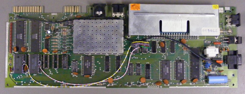
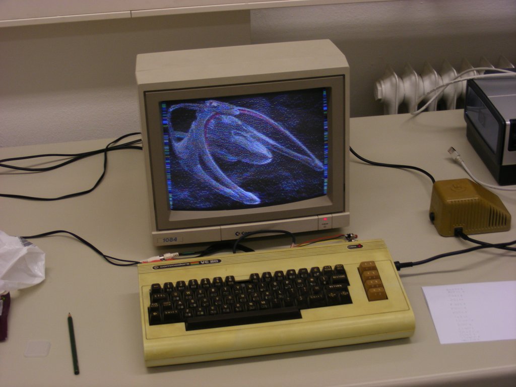
In the thread '** New Frontiers in VIC-Hires-Graphics, Part 10' I hinted at the possibility to expand the FLI mode presented there (72x256 pixels) to the full screen width of 208 pixels. This is possible with a hardware mod, I've done it, with great help from a friend with that extra experience in soldering work and of course electronics as well, to make this mod a success on the first shot.

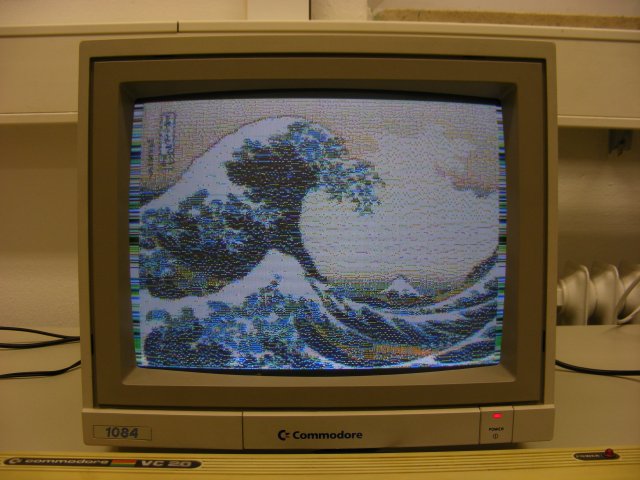
Here's the result. An image of Andromeda Ascendant - which was the first image tried out with the new display system:

Image

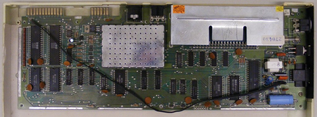
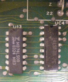
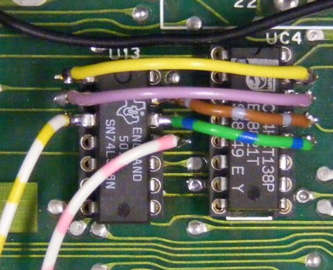
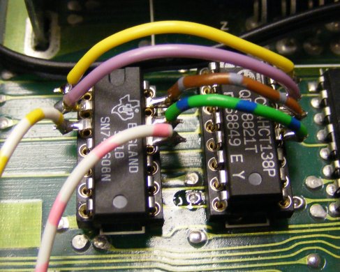
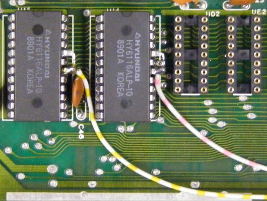
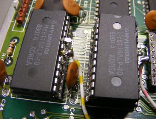
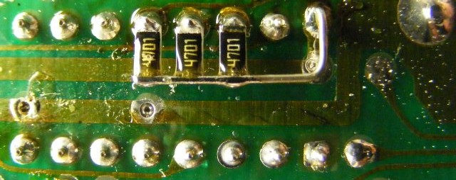
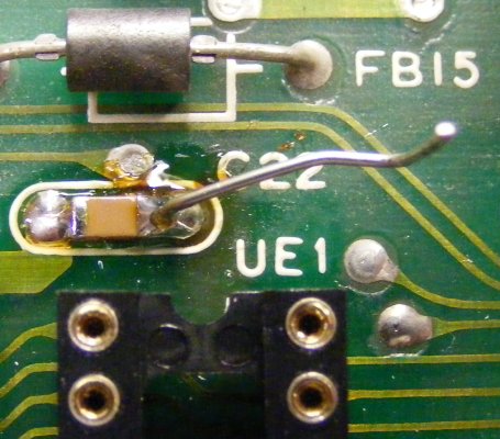
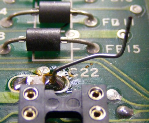
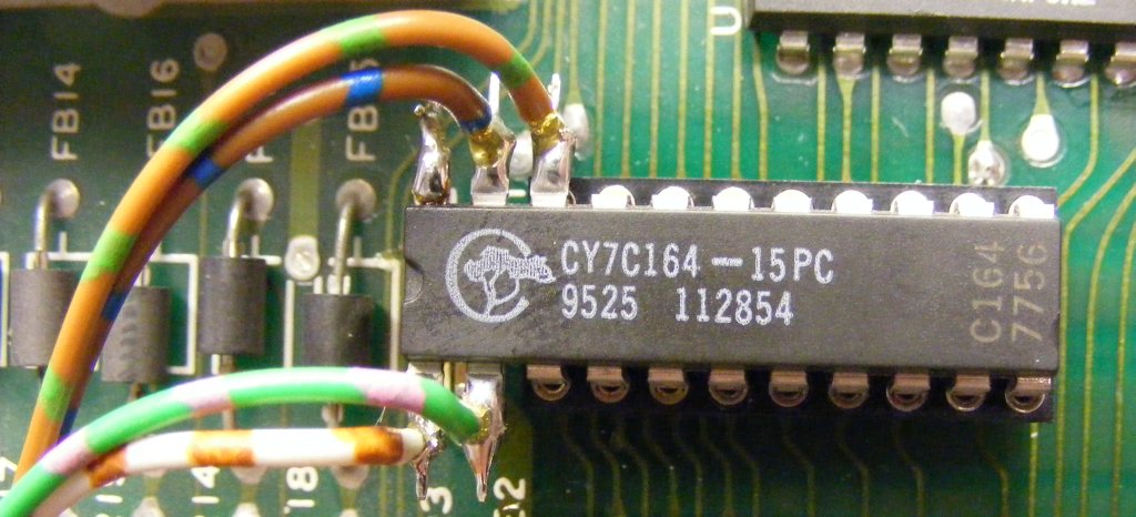
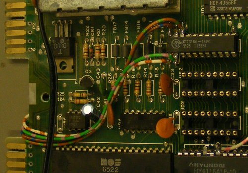
The hardware modification is done in 3 steps on a CR mainboard:

1. At first, all RAM chips and two chips of the select logic are desoldered, and sockets placed instead. This step completed, the chips can be re-inserted to check everything still works.

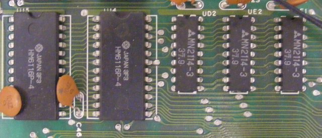
2. Internal RAM is expanded from 5K to 8K. This involves piggy-backing one extra RAM chip on the two existing 2K RAM chips and rewiring some part of the chip select logic. This also allows for an intermediary check.

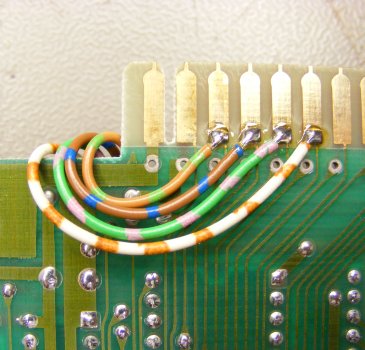
3. The colour RAM is replaced with a chip with 16 times capacity (i.e. 16K x 4 bits). The VFLI display routine then switches banks on each raster line to provide 8x1 attribute cells. The 4 necessary extra address lines are provided on the user port, with Port B of VIA1.

More details to the mod, and d/l links to two *.d64 images containing 30 images will follow shortly.

Cheers,

Michael
Last edited by Mike on Fri Nov 30, 2012 6:11 pm, edited 1 time in total.
grimm
Vic 20 Drifter
Posts: 22
Joined: Fri Nov 05, 2010 3:22 pm

Post by grimm »

Very cool! If the 64 had never came out I bet someone would have attempted this in the day. I'm looking forward to all of the details. :)
Grimm
User avatar
Mike
Herr VC
Posts: 4808
Joined: Wed Dec 01, 2004 1:57 pm
Location: Munich, Germany
Occupation: electrical engineer

Part 1: Socketing the RAM chips and select logic

Post by Mike »

First of all, the usual disclaimer: Do not perform this mod, unless you have a solid experience with soldering work. Also, take account of necessary ESD protect measures. I will not be held responsible if you damage your VIC.

My VIC is PAL, with a DIN power supply, and a CR (cost reduced) mainboard, all chips are soldered:

Image

The 5K of internal RAM and the colour RAM (1K nibbles) are located on the bottom left of above image, U15, U14, UD2, UE2, and UE1. Furthermore two chips of the chip select logic, U13 and UC4 are located just below the left edge of the expansion port connector:

Image Image

These seven chips need to be desoldered and replaced with a socket. Place the notch on the socket in the same orientation as indicated by the mounting print on the mainboard!

Doing this without damaging the chips and mainboard is possibly the most difficult part of the mod. You might ask a repair shop to do this job, though.

Reseat the original chips in their sockets. Again, note their orientation. If you switch on your VIC without any hardware expansions, it should greet you again with '3583 BYTES FREE'.

After that test, I kept the original chips as spares. Those set aside, you'll need the following parts to continue:

4x 6116 SRAM 2Kx8 (example: HY-6116ALP-10)
1x 74LS08 Quad-AND-gate
1x 74HCT138 3-to-8 inverting decoder/demultiplexer
1x CY7C164 SRAM 16Kx4 (replacement for UE1 2114 1Kx4 SRAM)
3x 4K7 SMD resistor 1206
1x 100 nF SMD capacitor 1206
some braided wire, and solid wire with a cross section of 0.25 mm².

The 6116 SRAM just needs to be faster than 400 ns, the replacement I used has a 100 ns cycle time - more than fast enough.
Last edited by Mike on Fri Nov 30, 2012 6:13 pm, edited 2 times in total.
Boray
Musical Smurf
Posts: 4064
Joined: Mon May 03, 2004 10:47 am

Post by Boray »

So you had to rebuild your computer to make your program work... ;) It's cool though...
PRG Starter - a VICE helper / Vic Software (Boray Gammon, SD2IEC music player, Vic Disk Menu, Tribbles, Mega Omega, How Many 8K etc.)
User avatar
nbla000
Salmon Run
Posts: 2582
Joined: Thu Oct 13, 2005 8:58 am
Location: Italy

Post by nbla000 »

But what about warranty ? :wink:
Mega-Cart: the cartridge you plug in once and for all.
User avatar
Mike
Herr VC
Posts: 4808
Joined: Wed Dec 01, 2004 1:57 pm
Location: Munich, Germany
Occupation: electrical engineer

Part 2a: rewiring the chip select logic

Post by Mike »

To expand the 5K internal RAM to 8K, it is necessary to rewire the chip select logic in U13 (74LS08) and UC4 (74HCT138).

UC4 generates the /RAM0, /RAM1, ..., /RAM7 signals (active low), which select 1 KB areas in BLK0, i.e. within the range $0000 to $1FFF. In the CR variant of the mainboard, /RAM0 drives a pair of 2114 1Kx4 SRAMs directly, providing the bottom 1K ($0000 to $03FF), while /RAM4 to /RAM7 are combined with U13 to form /CS and /OE for U15 and U14, realising the upper 4K (range $1000 to $1FFF). /RAM1 to /RAM3 go to the expansion port connector, and to UD9 which decides whether to separate the data bus between CPU and VIC chip. Two gates in U13 are unused.

These are the pinouts of the 74LS08 and 74HCT138 chips:

Code: Select all

      74LS08                 74HCT138
   +----\/----+            +----\/----+
1 -|A1     Vcc|- 14     1 -|A      Vcc|- 16
2 -|B1      B4|- 13     2 -|B      /Y0|- 15
3 -|Y1      A4|- 12     3 -|C      /Y1|- 14
4 -|A2      Y4|- 11     4 -|/G2A   /Y2|- 13
5 -|B2      B3|- 10     5 -|/G2B   /Y3|- 12
6 -|Y2      A3|-  9     6 -|G1     /Y4|- 11
7 -|GND     Y3|-  8     7 -|/Y7    /Y5|- 10
   +----------+         8 -|GND    /Y6|-  9
                           +----------+
At first, extract U13, U14, U15, UC4, UD2, and UE2 from their sockets again. UE1 is left in to facilitate easier testing when part 2 is complete.

You'll now need to bend straight the following pins:

U13 (74LS08): Pins 1, 2, 3, 11, 12, and 13;
UC4 (74HCT138): Pins 12, 13, 14, 15.

Now new 4 short braided wires connect UC4 and U13 to form new chip select signals for the ranges $0000 to $07FF and $0800 to $0FFF. Two long braided wires go to the places of U15 and U14. You should put the two chips in equal long sockets, so they can be held by a bench vice in the same relative position as they assume when put back to the mainboard again.

Solder the 4 short wires as follows ...

Code: Select all

UC4 Pin 15 -> U13 Pin 1   (former /RAM0 signal, yellow wire on photo)
UC4 Pin 14 -> U13 Pin 2   (/RAM1, violet)
UC4 Pin 13 -> U13 Pin 13  (/RAM2, grey-brown)
UC4 Pin 12 -> U13 Pin 12  (/RAM3, blue-green)
... and then solder two long wires to the remaining pins of U13:

Code: Select all

U13 Pin 3   (yellow-white, combined /RAM0 and /RAM1 for U15a)
U13 Pin 11  (pink-white, combined /RAM2 and /RAM3 for U14a)
The soldering process is probably made easier, if you "bend" the ends of the wires into small eyelets. Here's how it should look, when the chips are re-inserted into their respective sockets:

Image Image

Next to come: the four 6116 2Kx8 SRAM chips, piggy-backed.
Last edited by Mike on Fri Nov 30, 2012 6:15 pm, edited 1 time in total.
User avatar
orion70
VICtalian
Posts: 4337
Joined: Thu Feb 02, 2006 4:45 am
Location: Piacenza, Italy
Occupation: Biologist

Post by orion70 »

Mike, this is SO impressive... I was away for work and got back home now, and I guess I will study your mod tomorrow... even if I had a sneak peek of your new project in front of a good beer and a fine German dessert in Cologne :P .

Thanks for those stimulating new projects, which the brave could try to reproduce (even if they're definitely not for the faint at heart :wink: ).
Kananga
Vic 20 Afficionado
Posts: 317
Joined: Mon Mar 08, 2010 2:11 pm

Post by Kananga »

Impressive work. Sounds like you had a lot of fun.

The wires on the pictures look like they could stand 220V. Very robust design ;)
Buy the new Bug-Wizard, the first 100 bugs are free!
User avatar
Mike
Herr VC
Posts: 4808
Joined: Wed Dec 01, 2004 1:57 pm
Location: Munich, Germany
Occupation: electrical engineer

Part 2b: putting the 8K internal RAM into place

Post by Mike »

Thank you for all these kind replies! :) Of course the description of the mod isn't complete yet, but I hope to achieve this during the next day.

...

The part of the chip select logic, which has not been rewired is still in use, and selects U15 and U14 over conducting paths on the mainboard. Two further chips are soldered on top of U15 and U14 each - with the exception of two pins, which are connected to the newly generated signals from U13. The chips on top are dubbed 'U15a' and 'U14a'. I used four 6116 chips of the same batch. Here's the pinout of the 6116 2Kx8 SRAM:

Code: Select all

        6116
    +----\/----+
 1 -|A7     Vcc|- 24
 2 -|A6      A8|- 23
 3 -|A5      A9|- 22
 4 -|A4     /WE|- 21
 5 -|A3     /OE|- 20
 6 -|A2     A10|- 19
 7 -|A1     /CS|- 18
 8 -|A0    I/O8|- 17
 9 -|I/O1  I/O7|- 16
10 -|I/O2  I/O6|- 15
11 -|I/O3  I/O5|- 14
12 -|GND   I/O4|- 13
    +----------+
Both /OE and /CS need to be driven low so the chip outputs data on its I/O pins. In practice (and, certainly, on the VIC mainboard), they're simply connected to each other.

Before soldering U15a and U14a on top of U15 and U14, first bend straight their Pins 18 and 20. Then, carefully bend those two pins in the horizontal plane, so they contact each other. The result should resemble a small handle. Place a small tip of solder on the junction to connect them.

I'd recommend, that you first check that the bottom chips fit well into their sockets, so the insertion won't put additional stress on the solder joints. Now, put U15a on top of U15 (and likewise for U14a and U14), note that both notches are at the same end, and solder all remaining corresponding pins together. Check that you didn't miss out Pin 19. ;)

Insert the pairs into their sockets, then connect the chip select wires coming from U13, as follows:

Code: Select all

U13 Pin 3  -> U15a Pins 18, 20  (yellow-white wire)
U13 Pin 11 -> U14a Pins 18, 20  (pink-white wire)
The result should look like this:

Image Image

And here's an overview of the work done so far. Note the sockets of UD2 and UE2 will remain empty:

Image

This stage allows for an intermediary check: If you switch on your VIC without any hardware expansions, you should now already see '6655 BYTES FREE'. Even though, to complete part 2 of the mod, a small modification needs to be done on the solder side, to ensure that cartridges in the expansion port can't make trouble. Stay tuned. :)
Last edited by Mike on Fri Nov 30, 2012 6:17 pm, edited 1 time in total.
User avatar
e5frog
Vic 20 Nerd
Posts: 551
Joined: Sat Feb 17, 2007 5:46 pm
Website: http://channelf.se
Location: Sweden
Occupation: Service Engineer

Post by e5frog »

Button 7 is missing on that VC 20...

Interesting hack.

Is the best that can be done with a non-modified unit already done?
My other interest: http://channelf.se
User avatar
Mike
Herr VC
Posts: 4808
Joined: Wed Dec 01, 2004 1:57 pm
Location: Munich, Germany
Occupation: electrical engineer

Post by Mike »

Is the best that can be done with a non-modified unit already done?
As for graphics, for the unmodified VIC-20 there are MINIGRAFIK, MINIPAINT, MAXIGRAFIK, etc. available and well documented - feel free to actually use these programs.
User avatar
Mike
Herr VC
Posts: 4808
Joined: Wed Dec 01, 2004 1:57 pm
Location: Munich, Germany
Occupation: electrical engineer

Part 2c: disabling external 3K expansions

Post by Mike »

The original signals /RAM1, /RAM2 and /RAM3 on the mainboard are not anymore connected to and driven by UC4. On the one hand they are used by UD9 to separate the CPU and VIC data bus as necessary. Those inputs are now open, fortunately for the test in the preceding posting this doesn't matter, as floating TTL inputs are regarded as having high level by the respective gate - thus having no bad influence on the operation of UD9 in this case.

But on the other hand there might be other input gates for the RAM select lines on the other side of the expansion port. The open TTL inputs of UD9 place a signal level of ~2.4 volts on the RAM select lines, which is undefined for CMOS inputs! For that reason, it is necessary to put a well defined high level on the original /RAM1 to /RAM3 signal lines. This is done with three 4K7 SMD resistors connected to the original RAM select lines against the +5 V supply voltage, on the solder side, as shown below:

Image

You see the soldering side of UC4, and the expansion port faces to the right. The three resistors are soldered against pins 12, 13 and 14 of the socket, and the +5 V supply voltage is taken from pin 16 of the socket and connected via a solid wire to the other side of the resistors. The assembly actually "floats" roughly 1/2 mm over the mainboard.

Here's a small test program to check whether the RAM in the range $0600 to $1DFF is functional:

Code: Select all

1 POKE55,0:POKE56,6:CLR
2 X=RND(-2):FORT=1536TO7679:POKET,RND(1)*256:NEXT
3 X=RND(-2)
4 FORT=1536TO7679
5 IFPEEK(T)<>INT(RND(1)*256)THENPRINT"ERROR IN";T:STOP
6 NEXT
7 PRINT"ALL OK!"
This completes part 2 of the mod. It is now possible for the VIC chip to access the entire range of $0000 to $1FFF.

Part 3 will follow tomorrow.

Cheers,

Michael
Last edited by Mike on Fri May 10, 2013 3:22 pm, edited 2 times in total.
User avatar
Mike
Herr VC
Posts: 4808
Joined: Wed Dec 01, 2004 1:57 pm
Location: Munich, Germany
Occupation: electrical engineer

Part 3: Finale - replacing UE1 for more colours

Post by Mike »

Expanding the internal RAM from 5K to 8K already allows to display the 208x256 pixels mode of MAXIGRAFIK without any significant CPU usage. This frees up the 6502 for other tasks. It now can, for example, provide independent background/border and auxiliary colour on every raster. And FLI over the whole screen width is made possible by replacing UE1 with a chip of 16 times the capacity. Its 16 "banks" are switched on every raster, too - leading to 8x1 attribute cells!

Here are the pinouts of 2114 and CY7C164 in comparison:

Code: Select all

                              CY-7C164
                            +----\/----+
        2114             1 -|A5     Vcc|- 22
    +----\/----+         2 -|A6      A4|- 21
 1 -|A6     Vcc|- 18     3 -|A7      A3|- 20
 2 -|A5      A7|- 17     4 -|A8      A2|- 19
 3 -|A4      A8|- 16     5 -|A9      A1|- 18
 4 -|A3      A9|- 15     6 -|A10     A0|- 17
 5 -|A0    I/O1|- 14     7 -|A11   I/O3|- 16
 6 -|A1    I/O2|- 13     8 -|A12   I/O2|- 15
 7 -|A2    I/O3|- 12     9 -|A13   I/O1|- 14
 8 -|/CS   I/O4|- 11    10 -|/CE   I/O0|- 13
 9 -|GND    /WE|- 10    11 -|GND    /WE|- 12
    +----------+            +----------+
With the exception of 5 pins of the CY7C164, all others have a comparable function: /WE, /CE, GND, and most data and address pins are at the same place. For a SRAM chip it doesn't matter that the address and data pins are permuted in within their respective groups. Reading data back reverses any permutation in that case (this would not be true for EPROMs).

Pins 1, 2, 20, 21, and 22 of the CY7C164 need special treatment however. They're bent straight like done with UC4 and U13. To provide Vcc to pin 22, C22 on the mainboard needs to be desoldered, and a SMD capacitor of 100 nF and a solid wire on the +5 V side be soldered instead, so the wire can reach to the straightened pin 22:

Image Image

Now solder long braided wires to the pins 1, 2, 20, and 21 of the chip. These are the new address lines connected to the userport, as follows:

Code: Select all

Pin 1  <-> userport connector F (designated colour RAM address A13, brown-white wire on photos)
Pin 2  <-> userport connector E (new A12, pink-green)
Pin 21 <-> userport connector D (new A11, blue-brown)
Pin 20 <-> userport connector C (new A10, green-brown)
When the chip is inserted, with its bottom edge aligned to the bottom edge of the socket, solder pin 22 to the solid wire. That should look like this:

Image

The wires are guided to the right side of the userport (viewed with the userport facing away) and then soldered to the bottom end of the board connector row, on the soldering side of the mainboard, pins C to F:

Image Image

Congratulations! You're done. :D

The lower four bits of VIA1 port B (address $9110, decimal: 37136) now control the FLI bank. As long as the DDR register ($9112) is not initialised to 15, internal pull-ups in the NMOS variant of the VIA select bank 15 of the colour RAM. The banking is activated with POKE 37138,15. The bank then is selected with POKE 37136,x (x=0..15). Two *.d64 images with 15 images each in VFLI mode will follow shortly for you to try out the new hardware. :)
Last edited by Mike on Sun Jun 29, 2014 1:59 pm, edited 2 times in total.
User avatar
Mike
Herr VC
Posts: 4808
Joined: Wed Dec 01, 2004 1:57 pm
Location: Munich, Germany
Occupation: electrical engineer

Post by Mike »

So, here's vfli.zip (download). Below is another one of the 30 pictures stored in the two *.d64 image files:

Image

The viewer requires a PAL VIC-20 with above VFLI mod and an external 8K RAM expansion.

Source code of the display routine and a description of the VFLI file format have been included as well.

Greetings,

Michael
Last edited by Mike on Thu Feb 20, 2014 4:16 pm, edited 2 times in total.
User avatar
e5frog
Vic 20 Nerd
Posts: 551
Joined: Sat Feb 17, 2007 5:46 pm
Website: http://channelf.se
Location: Sweden
Occupation: Service Engineer

Post by e5frog »

How long does it take to load and display the picture?
My other interest: http://channelf.se
Post Reply