6561 Die Shot Reversing Explorations

Modding and Technical Issues

Moderator: Moderators

lance.ewing
Vic 20 Afficionado
Posts: 413
Joined: Sat Nov 10, 2012 3:19 pm
Website: https://sites.google.com/site/mos6561vic/

Re: 6561 Die Shot Reversing Explorations

Post by lance.ewing »

lance.ewing wrote:The POT_X input on the left has come from a section of the die shot that we haven't looked at yet, but it comes from the direction of the POT X bonding pad after having passed through some circuitry that currently I'm a bit perplexed by (I'm wondering if it relates to the amplifier symbols on the block diagram).
Over the last few posts, we've been looking at the digital side of the POT analog to digital converters. In reference to the above quote, the reason I was perplexed by the section of the die shot that the POT_X signal is coming from is because it's analog in nature. Up until this point, the vast majority of the sections of die shot we have been looking at have been digital logic. Over the past couple of years, I've become quite familiar with recognising digital structures, but not analog. Electronics being a hobby for me, and digital being the primary focus, I don't have a good understanding of the analog side.

But despite my lack of experience, we already have a fair idea of what to expect with the 6561 POT ADC circuits. We can start with what the datasheet tells us:
These input pins are used to convert potentiometer position into a microprocessor readable 8 bit HEX number. This is accomplished by a simple RC time constant integration technique. The potentiometer is used to charge an external capacitor tied to the pot pin.
(Emphasis added)

So this tells us that the integration is a simple RC time constant mechanism, and that the capacitor is external. A simple RC integrator looks like this:
rc20.gif
rc20.gif (3.8 KiB) Viewed 8486 times
(source: https://www.electronics-tutorials.ws/rc ... rator.html)

...as a lot of you will already be very familiar with. And this diagram looks like what we have connected to the 6561 POT pins on the VIC 20 circuit board when a paddle is connected to the joystick port. Obviously without the paddle connected, it isn't an RC integrator. The capacitor is on the VIC 20 circuit board, and the variable resistor in the paddle.

I found the following article that is worth a read. It describes a mechanism for using a digital input to an MCU to read an analog signal. All it uses is an RC integrator circuit, and the MCU counts how long it takes the digital input to go HIGH, and then discharges it by pulling the pin low.

https://www.microcontrollertips.com/mcu ... thout-adc/

I've been reading up on ADC designs over the past few days, and the design that seems closest to what we see with the 6561 is the single slope ADC. I've discounted the dual slope ADC because there doesn't appear to be anything that switches between a Vin and Vref. The Vref is internal to the 6561 (in fact I believe I've identified where it is generated) and we just have the input coming in. This input though is the input after the RC integrator (keep this in mind when looking at the next diagram).

A single slope ADC is usually shown to look something like this:
317_101.gif
(source: https://www.hardwaresecrets.com/how-ana ... c-works/8/)

I was a bit hesitant to include the above diagram, because it isn't quite what is happening with the 6561. I couldn't find a closer match though. Instead let's view the above as a more classic single slope ADC as a means to introduce the concept. The diagram above shows the Vref being used with the integrator, but in the case of the 6561, it seems that the integrator (the RC integrator mentioned above) is used with the Vin. Instead the internally generated Vref within the 6561 seems to be one of the direct inputs to the comparator, and is fixed, whereas the Vin goes through the external RC integrator and then into the internal comparator.

It is worth talking a bit about the simple slope ADC diagram above. The box labelled "Output Buffer" is the equivalent of the 6561 POTX or POTY register (CR8 and CR9) and the Counter is the 8-bit counter that we have already identified in the 6561. We can see from the diagram that there is a clock signal that increments the Counter. When the comparator output changes, it clocks the transfer of the current Counter value into the lower box. The diagram above also shows the comparator clearing the Counter, but this isn't what happens in the 6561. Instead the counter will keep counting up to its maximum value (at which point it stops counting) and will reset when the vertical counter is next at a multiple of 8. The above diagram also shows the comparator change in output discharging the capacitor, but in the 6561 that doesn't happen and instead it is likewise discharged when the vertical counter is next at a multiple of 8.

Remember, the 6561 is using an external RC integrator rather than a op amp integrator. On every 8th line, it pulls the POT pin low to discharge the external capacitor.

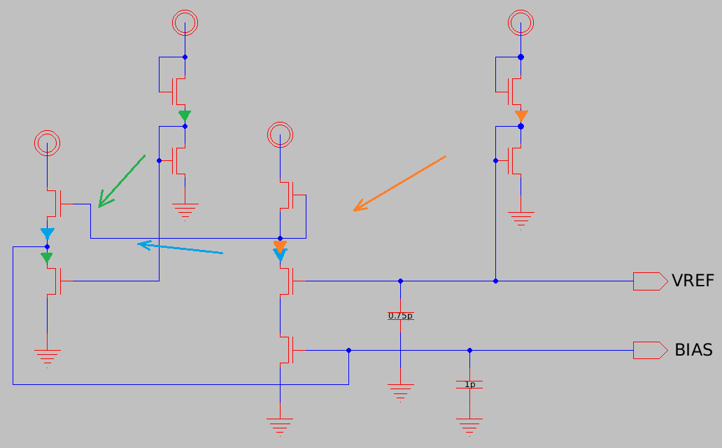
In the next post, we're going to start looking for the comparator, which will involve identifying differential pairs, a constant current source, and reference voltage (Vref).
User avatar
beamrider
Vic 20 Scientist
Posts: 1452
Joined: Sun Oct 17, 2010 2:28 pm
Location: UK

Re: 6561 Die Shot Reversing Explorations

Post by beamrider »

excellent work - I don't have much to add but keep following along. Looking forward to the day, when the chip can be recreated.
lance.ewing
Vic 20 Afficionado
Posts: 413
Joined: Sat Nov 10, 2012 3:19 pm
Website: https://sites.google.com/site/mos6561vic/

Re: 6561 Die Shot Reversing Explorations

Post by lance.ewing »

Kakemoms wrote:Just to update: I have been working and traveling a lot so didn't finish the pictures of the 6560. That being said, we now have a new 3D optical microscope in the lab, so I want to take some pictures with that before we move out of here.
That would be really great. I would like to spend some time looking more closely at the 6560 at some point. I have noticed from what you've posted already that the POT related circuitry appears to be different than in the 6561. I'm basing this mainly on the shapes in this area of the die. It is clear that there are quite a few differences, but I won't be able to tell what they are until we have some clear optical images of that area.

While you are at it, could you measure the width of one of the normal width metal lines? So not the ones that get really fat in places, but the standard metal lines, which I guess is the minimum width metal line. I can work out a ball park figure from some of the images you posted, but it would be great to get an exact measurement. Maybe a measurement of the diameter of a metal to diffusion contact as well, which actually looks to be about the same width as the metal lines.

Where I'm trying to get to is what the value of lambda might be for the 6560/1. The Mead/Conway book mentions in the design rules section that, at that time, a metal line was 3 lambda wide and would be no closer to another metal line than 3 lambda. There are various other rules based around the value of lambda. So I was wondering what it might be for the 6560/1 chip.
lance.ewing
Vic 20 Afficionado
Posts: 413
Joined: Sat Nov 10, 2012 3:19 pm
Website: https://sites.google.com/site/mos6561vic/

Re: 6561 Die Shot Reversing Explorations

Post by lance.ewing »

I just found a very interesting and relevant chapter from an online copy of the book "The Computer Controller Cookbook" this evening. The book was published back in 1983. It validates a lot of what we covered in my post from a few days ago:

https://www.atariarchives.org/ccc/chapter14.php

Here is the relevant image from this book:
fig14-1.gif
fig14-1.gif (6.92 KiB) Viewed 8411 times
And this is a related quote discussing this image:
Drawing 14-1 shows how the timer is controlled. When the timer is started, the capacitor is discharged and then allowed to recharge through the resistor in the controller. The resistance of the controller is dependent on the setting of the mechanical knob. The lower the resistance, the faster the capacitor can charge, so less time is available for the computer to count. When the amount of resistance in the controller is high (i.e. the controller is at its highest setting) the capacitor will charge to the trigger reference voltage more slowly, allowing the timer's counter to reach a higher value before the timer is tripped. When the trigger reference voltage (about 1.7 volts) set in the design of the timer is reached, the timer is tripped and sets a flag so that the computer will stop counting. This length of time is controlled by the product of the capacitance times the resistance of the controller.
Interesting what it says about the trigger reference voltage. That page refers to four different computers but makes a statement like that that seems to imply that the reference voltage would be the same for all of them. Not sure if that would be true, but something to keep in mind. It also mentions that the VIC 20 paddles use 1 meg-ohm pots, but from diagrams I've seen elsewhere, it seems to be 470 ohms instead.
lance.ewing
Vic 20 Afficionado
Posts: 413
Joined: Sat Nov 10, 2012 3:19 pm
Website: https://sites.google.com/site/mos6561vic/

Re: 6561 Die Shot Reversing Explorations

Post by lance.ewing »

Another interesting related bit of reading, this time from a review of using three different paddles with a C64:

http://www.breadbox64.com/blog/paddle-battle/

It includes the VIC 20 paddles and the Commodore Model 1312 paddles. Both claim to be 470kΩ, but the reviewer measured the VIC 20 one as 625kΩ. It is also interesting what it says about the 'sensitivity', or how many degrees between the minimum and maximum pot register values (i.e. 0 and 255). I had been labouring under another bad assumption that the pot reg would reach 255 at 470kΩ, but apparently it could be quite a lot less. For the VIC 20 paddles, the reviewer measured the 'sensitivity' at 100° on a C64, despite the fact that the pot knob could turn 300°.

I think I need to build myself a small paddle so I can measure what the pot resistance is just as the pot register changes from 254 to 255. I have now simulated the analog part of the 6561 pot circuit but it assumes a reference threshold of 2.5V. With that threshold, about 436 cycles pass when it is triggered with the pot set to 470kΩ. I need to work out what the actual threshold voltage is on the real machine.
User avatar
srowe
Vic 20 Scientist
Posts: 1340
Joined: Mon Jun 16, 2014 3:19 pm

Re: 6561 Die Shot Reversing Explorations

Post by srowe »

lance.ewing wrote: Interesting what it says about the trigger reference voltage. That page refers to four different computers but makes a statement like that that seems to imply that the reference voltage would be the same for all of them. Not sure if that would be true, but something to keep in mind. It also mentions that the VIC 20 paddles use 1 meg-ohm pots, but from diagrams I've seen elsewhere, it seems to be 470 ohms instead.
The "VIC Revealed" claims they're 100K...
lance.ewing
Vic 20 Afficionado
Posts: 413
Joined: Sat Nov 10, 2012 3:19 pm
Website: https://sites.google.com/site/mos6561vic/

Re: 6561 Die Shot Reversing Explorations

Post by lance.ewing »

lance.ewing wrote:I think I need to build myself a small paddle so I can measure what the pot resistance is just as the pot register changes from 254 to 255.
It looks like @Schema did a similar test many years ago:

http://sleepingelephant.com/ipw-web/bul ... 6744#p6744
Schema wrote:I just measured the resistance of my (jittery) Atari paddles on my VIC. I did a PEEK(36872) repeatedly to get the recognized range. Then I unplugged the paddles before measuring the corresponding resistances, so I wouldn't get a voltage division across the VIC innards.

The VIC recognized the range between 0 Ohms (=0) and slightly under 300 Kohms (= ~255). The paddles went up to a maximum of 900 Kohms.
This might already tell me what I need to know. I'll start thinking about it.
lance.ewing
Vic 20 Afficionado
Posts: 413
Joined: Sat Nov 10, 2012 3:19 pm
Website: https://sites.google.com/site/mos6561vic/

Re: 6561 Die Shot Reversing Explorations

Post by lance.ewing »

srowe wrote:The "VIC Revealed" claims they're 100K...
I think that diagram on page 217 (Fig 37) is wrong. It also shows the cap as 0.1uF, which doesn't match what is on the VIC 20 board.
lance.ewing
Vic 20 Afficionado
Posts: 413
Joined: Sat Nov 10, 2012 3:19 pm
Website: https://sites.google.com/site/mos6561vic/

Re: 6561 Die Shot Reversing Explorations

Post by lance.ewing »

In this post we'll be looking at the part of the 6561 die shot where the POT analog comparators lie, as highlighted by the pink box in the following image of the die shot:
pot_comparators_highlighted.jpg
The two bonding pads are immediately above the pink box. A close up of those bonding pads was shown in an earlier post when discussing the pull down transistor controlled by the EVERY_8TH_LINE signal. I have drawn the pink box split into three sections. In the right section is the POTX comparator, in the middle section the POTY comparator, and on the left is the reference/trigger voltage generation and bias generation for the comparators. This post will be focusing mainly on the POYX comparator section. The following image shows a close up of that section:
pot_x_comparator.jpg
If you open that image in another tab, and then look up near the top right corner, you'll notice two polysilicon lines, one that is labelled POTX and one that is labelled VREF. Those are the inputs to the POTX comparator. The POTX line comes from the POTX bonding pad, and the VREF line comes from the reference/trigger/threshold voltage generation section. You will notice that there are three parts of this image that look a bit similar. The following shows a close up of the two of these:
pot_x_differential_pair_close_up.jpg
These two structures that have the long vertical red polysilicon lines through the middle of them are what is known as differential pairs, or long tailed pair, and are a type of differential amplifier:

https://www.allaboutcircuits.com/techni ... tial-pair/
https://wiki.analog.com/university/cour ... chapter-12

One of the distinguishing things about them is that the source of the two transistors (whose gates have the inputs connected to them) are connected to each other, and then that shared connection point is then connected to a constant current source.

https://www.allaboutcircuits.com/techni ... nt-source/

We see exactly the structure of a different pair when reversing from the silicon. The full schematic for the POTX comparator section looks like this:
potx_comparator_schematic.png
...where the BIAS input shown is connected to a constant current source similar to those shown in the article above, and the VREF input is connected to a simple voltage divider. We'll look more closely at that section of the die shot (i.e. the left part of the pink box) in another post. For now we'll look at the part of the circuit that we see above. For the differential pairs, depletion mode transistors are used for the pull ups (rather than resistors, which take far too much space). The schematic shows three differential pairs with what appears to be a type of inverting buffer between them. Then after the third differential pair, i.e. the one on the left, there is a type of latch. There will be people reading this that will understand the circuit much better than I do, but I've simulated it in a tool called Proteus and it does what you would expect it to do from a black box perspective, i.e. the POTX_COMP_OUT signal goes high when the POTX voltage hits the threshold/trigger/reference voltage.

This POTX_COMP_OUT signal is the input to the POTX load logic that we looked at in an earlier post. In that previous post it was called simply POTX, but now we can see (and we probably anticipated this anyway) that it is the output of the POTX comparator.

Obviously the POTY comparator works in exactly the same way, and has the same VREF and BIAS inputs, but with the POTY input rather than POTX, and with a POTY_COMP_OUT output.
User avatar
Mike
Herr VC
Posts: 4841
Joined: Wed Dec 01, 2004 1:57 pm
Location: Munich, Germany
Occupation: electrical engineer

Re: 6561 Die Shot Reversing Explorations

Post by Mike »

Hi, Lance!

This looks like you're homing in on the Paddle Jitter Issue. :)

As for the function of the comparator circuit -
lance.ewing wrote:There will be people reading this that will understand the circuit much better than I do [...]
In principle, the three differential pairs act as discriminators - they amplify the voltage difference of their input but (mostly) reject a common mode, i.e. their output doesn't change much if both voltages are increased by the same amount.

They do this by a deceptingly easy method: the current of the constant current source (the biased FET at the bottom) goes to both differential FETs, and what current goes to the left FET can't go to the other. :) So, if you imagine these two FETs as valves, and have two equal flows going through both; when one then "opens" the valves by the same amount - nothing changes! Finally, the current(-difference) gets "converted" to a voltage(-difference) on the output simply by producing a voltage drop at the pull-ups. Now for itself, each half of the differential pair isn't much more than a source follower, so you get mostly a impedance transformation (and the common mode rejection) but no (big) amplification as such.

This amplification is provided by the two doubled in-between totem-pole stages. They increase the slope of the incoming ramp, so where the POT% inputs provide something that increases by, say, 0.01 Volts/µs, these two stages may provide an amplification of 50 each, and end to end, which gives around 25 Volts/µs for the last stage, or rather, just ~200 ns for the the differential voltage to swing between ~0 Volts on one side and ~+5 Volts on the other - or the other way round.

The last structure on the left are two differential pairs with a twist - their current source is switched! This makes up for something much resembling a flip-flop, but it has a hysterese on its input, so "just" going back to the middle doesn't suffice to make it flip (what you correctly describe as latch). If there is any ringing on the (amplified) signal, this structure isolates this from the rest of the chip logic. So under *ideal* conditions, POTX_COMP_OUT just works as you describe.


Now for the non-ideal conditions:

- Normally, a differential pair gets its constant current from a structure, where the common FET is part of a current mirror. The current source can only be as good, as both FETs of the current mirror are tightly coupled, electrical and by temperature. If BIAS goes over a lengthy connect, other signals can couple into it.

- Providing VREF "just" from a voltage divider is just, well, erm.

- What's mostly intriguing: the reference/trigger generation and bias generation should have been placed symmetrically, *between* the POTX and POTY comparators! As it is here, POTX gets its VREF and BIAS signals only after they had "wound around" the POTY section. So, whatever makes the POTY comparator bad already, doesn't get better when VREF and BIAS pick up noise from the POTY comparator and then serve the POTX comparator ...


Edit: possibly I need to revise the latter part of the criticism a bit: it's actually POTY that suffers more from jitter (see the Paddlescope thread). Possibly, the proximity to switched signals (POTY -> EVERY_8TH_LINE, etc.) plays a slightly bigger role here than the more lengthy signal paths for POTX. Still ...

Just for a cross-check: you had arranged the three boxes in the order: switching/threshold/bias, POTY, POTX and this corresponds well to the pinout of VIC-I (if one imagines the chip die is turned 90° to the left before being bonded).
lance.ewing
Vic 20 Afficionado
Posts: 413
Joined: Sat Nov 10, 2012 3:19 pm
Website: https://sites.google.com/site/mos6561vic/

Re: 6561 Die Shot Reversing Explorations

Post by lance.ewing »

Thanks Mike. That fills a lot of the gaps in my explanation. I was hoping someone would pick it up and help describe what is happening. I'm glad that it makes some sense. Hopefully I haven't put you wrong with the VREF and BIAS parts of it. I'm going to cover that in a bit of detail below. For me there are still a lot of question marks about it, and I may have made some assumptions that aren't correct. So let's take a closer look...
Mike wrote: - Normally, a differential pair gets its constant current from a structure, where the common FET is part of a current mirror. The current source can only be as good, as both FETs of the current mirror are tightly coupled, electrical and by temperature. If BIAS goes over a lengthy connect, other signals can couple into it.
It does seem to be quite a lengthy connect, and it does pass through all the POTY bias FETs before it starts passing through the POTX bias FETs. In the case of the POTX bias FETs, they are all transistors with a straight shape, but in the case of the POTY bias FETs, they are all weaving around a bit (like what an NMOS register would normally do), which I assumed was because there wasn't as much space on the die in that area as there is for the POTX bias FETs. The following diagram shows both sets of FETs showing also the long line that passes through them, highlighted in cyan (it starts on the far left, where it is connected to a capacitor that is not quite in the image):
poty_and_poyx_bias_fets.jpg
I could be wrong, and perhaps they're not bias FETS. It seems to make sense for where they are though. The diagrams I've seen for differential pairs show either a constant current source or a high value resistor. So I've assumed that these FETs must be part of a constant current source. Unfortunately I really struggled to work out whether what they are connected to does behave like a current source. Hopefully you can help me out with this. Let's start with a close up of the left hand section of the pink box (i.e. VREF and BIAS section):
bias_and_ref.jpg
This is what I think the schematic for the above looks like:
pots_bias_and_vref_schematic.png
pots_bias_and_vref_schematic.png (10.01 KiB) Viewed 8262 times
But I'm by no means 100% certain of this schematic, because some parts of it were difficult to spot whether there was any buried contact, and certainly the implant that would make a transistor into a depletion mode transistor is almost always impossible to see. When I'm reversing the digital logic gate parts of the 6561, I know the implant must be there, because the NMOS depletion load fabrication used by the 6561 uses depletion mode transistors for the logic gate pull ups. When it comes to the analog parts of the circuit, I can't really tell whether the pull up transistors are depletion mode or the normal enhancement mode transistors. I've assumed in the above schematic that they're all enhancement mode transistors, mainly because they don't look like what I'm used to with depletion mode transistors. It could be that one or more of those pull ups are depletion mode.

If you think there is something not quite right with the circuit, and that it would function better with a tweak here and there, then it is quite possible that the 6561 has those tweaks and I just couldn't see them. I would be very interested in knowing your feedback on this circuit. One thing that the above schematic doesn't show is the dimensions of the transistors. Although there are two pull up/pull down pairs that look identical (i.e. with the top transistor connected to VSS, and the bottom transistor's gate connected to its drain), the one that has its output connected to the VREF line has transistors of exactly the same dimensions, but the other similar transistor pair has transistors of different dimensions.

In my simulation, I couldn't get this circuit to function as a constant current source, and so I simplified it to the examples I'd seen online for what a basic constant current source would look like. That made the differential pairs work in the simulation, but it raises a number of questions: The first is whether the above schematic for the constant current source is correct, which I have several doubts about. And another question is whether those FETs at the bottom of the differential pairs really are part of a constant current source. I'm still assuming they are, because it seems to make sense, and I've read several articles online that say integrated circuits would normally always use a constant current source for a different pair (rather than a resistor).
Mike wrote: - Providing VREF "just" from a voltage divider is just, well, erm.
I am hoping that I haven't put you wrong there. To me it looks like it could be a simple voltage divider circuit, but I did struggle to spot some of the connections that I assume are there. The reason I've done well so far with the parts of the 6561 that are primarily logic gates is because when I can't quite see the buried contacts, I can assume that they would be there. But with these analog structures, I'm not so sure what to expect. So let's have a close up look at what I think is providing the VREF value:
vref_closeup.jpg
Although the lines I have drawn might not make those transistors look exactly the same dimensions, I've done a few measurements and I'm fairly sure they are of the same dimensions, i.e. same width and length, and therefore the same resistance. I've assumed that there is a buried connection from the lower transistor's gate and the point between the two transistors, i.e. a gate to drain connection for that lower transistor. The reason I have assumed it is there is because otherwise there isn't anything connected to that gate. I've followed all other paths to that gate and there is nothing else providing an input, so there has to be a connection from the gate to the drain. There are hints in the die shot image that it is there, so my best guess is that it is there. And if this is the case, then it seems that with VDD at 5V, then the output is at 2.5V, which is what feeds the VREF signal. I've simulated two identical transistors connected in this way and the output is 2.5V. This is why I've assumed that the threshold voltage is 2.5V.

Can you confirm that this is a voltage divider? Or does such an arrangement of MOSFETs have a different name? - If it is a voltage divider, then can you explain further why this seems unusual by itself?
Mike wrote: - What's mostly intriguing: the reference/trigger generation and bias generation should have been placed symmetrically, *between* the POTX and POTY comparators! As it is here, POTX gets its VREF and BIAS signals only after they had "wound around" the POTY section. So, whatever makes the POTY comparator bad already, doesn't get better when VREF and BIAS pick up noise from the POTY comparator and then serve the POTX comparator ...
Yes, it does seem that it should ideally be placed between the two.
Mike wrote: Edit: possibly I need to revise the latter part of the criticism a bit: it's actually POTY that suffers more from jitter (see the Paddlescope thread). Possibly, the proximity to switched signals (POTY -> EVERY_8TH_LINE, etc.) plays a slightly bigger role here than the more lengthy signal paths for POTX. Still ...
I have read over your Paddlescope thread a number of times, and will probably do so a few more times in the future. I was wondering, given the apparent influence by the VIC chip's fetching of data when within the text window, were you able to prove that when you read the POT values outside of the text window, that the jitter was not present?
Mike wrote: Just for a cross-check: you had arranged the three boxes in the order: switching/threshold/bias, POTY, POTX and this corresponds well to the pinout of VIC-I (if one imagines the chip die is turned 90° to the right before being bonded).
I checked this a few times as well. The bonding pads around the outside of the die shot do appear to be in the same sequence as the pinout for the 6561. I've also tracked the paths through from those bonding pads through to the corresponding VIC registers, and then checked the address decoding logic for the two registers, and I'm fairly sure from that end that the two comparators have been identified correctly.

Well I've just spent most of the afternoon typing this post up, with one eye on the England vs Sweden game (I'm not English, but I do live in England, and my home country only makes it to the World Cup every quarter century!, so I have to pick someone to support!). - I'll click the submit button now before I lose this text.
lance.ewing
Vic 20 Afficionado
Posts: 413
Joined: Sat Nov 10, 2012 3:19 pm
Website: https://sites.google.com/site/mos6561vic/

Re: 6561 Die Shot Reversing Explorations

Post by lance.ewing »

lance.ewing wrote:
Kakemoms wrote: Really interesting development! Are you ready to put it into Verilog yet.. (I know, its a tedious language!) If you want me to put some short routines into verilog, I can certainly manage.
I think when I return to using Lattice Diamond, I'll focus on implementing things in Verilog. I think Lattice Diamond wasn't suited to the goals I had when I began using it. I was looking for a tool that would allow me to draw logic diagram type schematics for what I'd worked out, like what I was doing in Logisim, which I could then simulate. I ran into problems with the schematic drawing tool in Lattice Diagram. Things got a bit ridiculous when I was trying to lay out the X decoder. I kept thinking "This would only be a few lines in verilog".

So maybe Logisim, or something simple like that, would be best for creating logic diagrams, and in Lattice Diamond I'll stick to verilog.
I know this sounds bad, but I had nearly forgotten that I purchased a license for a tool called Proteus back in 2015. This is before I began reversing the 6561 die shot. Back then I certainly had an interest in the 6561 die shot, and spent hours here and there staring at the image, but I hadn't begun to draw around the various types of material until 2016. In 2015, I was playing around with a 4-bit home brew CPU on a breadboard. I simulated the whole thing in Proteus. Prior to that I had tried simulating it in Logisim, but for some reason it didn't work. It wasn't until I bought a license for Proteus, and created the schematic in that tool, that I was able to successfully simulate the 4-bit homebrew CPU.

Why am I relating this story? Well it seems that I almost forgot that I'd bought a license for Proteus back in 2015. When I began reversing the 6561 chip in 2016, I was using Logisim quite a lot, because most of it was logic gates and Logisim was well suited to that. When I became unstuck with Logisim when attempting to simulate everything I'd learnt so far, I didn't remember even for one second that I had a License for Proteus. This might be because my desktop PC is a Debian Linux PC and I run Windows within VirtualBox. I had lost my VirtualBox machine image that had Proteus installed on it and I never got around to reinstalling it when I got the VM back up and running again.

But now I have, and I'm now remembering how easy it is to use Proteus. Everything just seems to work as I would expect. So I'm planning to start building up a simulation of the whole 6561 chip within Proteus over the next month or so, starting with the clock generation circuits, which is always a good place to start. :)

I will eventually put it into Verilog and Lattice Diamond, but for now I want to try out something that I'm familiar and comfortable with. Proteus has a 320x200 colour LCD component that I'm eyeing up as an output for the pixel output in the simulation.
User avatar
Mike
Herr VC
Posts: 4841
Joined: Wed Dec 01, 2004 1:57 pm
Location: Munich, Germany
Occupation: electrical engineer

Re: 6561 Die Shot Reversing Explorations

Post by Mike »

lance.ewing wrote:The diagrams I've seen for differential pairs show either a constant current source or a high value resistor. So I've assumed that these FETs must be part of a constant current source. Unfortunately I really struggled to work out whether what they are connected to does behave like a current source.
The current mirror I referred to in my preceding post produces such a current source, provided there is enough voltage on the second transistor/FET to drive that current (warning: ASCII art):

Code: Select all

I
 in
                       I
 |                      out 
 V                       
 |                       |
 |                       V
 |                       |
 o-----------+           |
 |           |           |
 |           |           |
 |           |           |
 +---+ |     |     | +---+
     | |     |     | |
     | o-----o-----o |
     | |           | |
 +---+ |           | +---+
 |                       |
 |                       |
 |                       |
-o-----------------------o- GND
Whatever I_in is applied as input, it drives/charges the gate of the left FET in a way so it lets it pass - exactly this gate voltage is also applied to the right FET, so that one is supposed to sustain an equal source-drain current. [1] What makes this simple construct valuable is the high differential resistance of the right FET: one can change the voltage over the right FET by quite some amount without changing the current (one can think of this differential resistance as being a parasitic element in parallel to the source-drain channel of the FET, or the emitter-collector terminals of a BJT).

With FETs, this circuit works remarkably well, as the two gates doesn't place any (static) load on I_in. With BJTs, this variant of the current mirror is also slightly dependent on their amplification B, you get I_out = B/(B+2) * I_in in this case: I_C = B * I_B, I_in = I_C + 2 * I_B (I_in has to drive both bases!) I_out = I_C. For BJTs, there exists a cascaded version of the current mirror with better characteristics, but this not normally necessary for the FET version.


The signal you named BIAS would be exactly the connection from the gate of the left FET to the right FET; and the common FET of the differential pairs then is supposed to be the right FET. Trouble is, while I can make out three current mirrors in your schematics (see the arrows in my annotated version below, I_in is right, I_out is left for all mirrors), none of them connect to BIAS as I'd expect. Rather, they seem to be part of a bootstrap or compensation network:

Image

1. The "green" current mirror works on its own and makes the left-most bottom FET drain the same current as the pull-up.
2. BIAS itself is not expected to have *any* relevant current.
3. Thus, the light blue current (left) must supposedly be the same as the green current (left).
4. Which requires, that the light blue current (right) is equal to the pull-up current (green right).
5. which is however flowing through two FETs whose gates are controlled by VREF and BIAS. :shock:

Now it's gonna be floundering... the voltage divider for VREF actually supplies the necessary bias voltage for the light blue input current, but only if the lower of the two FETs (with its gate connected to BIAS) has a very low resistance, so the upper of the two FETS (with its gate connected to VREF) acts as output of a (well hidden) third current mirror (orange current arrows). If, for some reason, the lower FET (BIAS gate) blocks some or all current, its gate is *discharged* by the green current (left arrow) - it needs to be a depletion mode FET so this would work at all (i.e., assume a non-0 BIAS voltage). I can't even rule out *oscillatory* behaviour here, something like a charge pump for the lower capacitor.

In any case, with BIAS then meandering around and serving six FETs for the common current of the differential pairs isn't exactly what I'd expect, even given there's an extra decoupling capacitor. If there's any switched signal nearby, this calls for trouble.

Can you confirm that this is a voltage divider? [...] If it is a voltage divider, then can you explain further why this seems unusual by itself?
It is a voltage divider for VREF, sure. A bandgap reference would be an alternative. Though it's probably better to have an explicit ratio of Vcc here, rather than some fixed voltage.

A lot of open ends at the moment, for sure.

were you able to prove that when you read the POT values outside of the text window, that the jitter was not present?
For the big spikes, their duty time is more or less exactly the same time no DMA is done. If they were coupled to the VBLANK period, they'd only be half as wide. If I find time next week, I can re-check on real h/w that these spikes exactly correspond to the non-DMA time.

Greetings,

Michael


[1]: both FETs need to share the same geometry, have the same temperatur, and the connect between the two gates needs to be as small as possible.
lance.ewing
Vic 20 Afficionado
Posts: 413
Joined: Sat Nov 10, 2012 3:19 pm
Website: https://sites.google.com/site/mos6561vic/

Re: 6561 Die Shot Reversing Explorations

Post by lance.ewing »

This evening I'll only get a chance to add the following version of the VREF and BIAS schematic with the dimensions of the various transistors shown, the width being the top number, and the length the bottom number:
pots_bias_and_vref_schematic_2.png
I've read that the resistance of these transistors is about 10K per square. The number of squares is Length/Width. So in the example of the lower FET with 17 as a width and 1 as the length, the resistance would therefore be about 10000/17 or approximately 588 ohms.

The FET that we suspect might be a depletion mode transistor (and that I have now changed to depletion mode) has its dimensions obscured in the above image. The dimensions are exactly 1 by 1 for that one.

I intend to post some even closer up die shot images of these FETs later this week, drawing attention to various features that may or may not be important.
lance.ewing
Vic 20 Afficionado
Posts: 413
Joined: Sat Nov 10, 2012 3:19 pm
Website: https://sites.google.com/site/mos6561vic/

Re: 6561 Die Shot Reversing Explorations

Post by lance.ewing »

Here is another version of the schematic with the various points labelled:
pots_bias_and_vref_schematic_3.png
And this is an image of the area of the die shot showing where these same points are, labelled with the same colours and letters:
bias_and_ref_points_labelled.jpg
We can see from this that the connection from point D (the gate of transistor labelled D) and point G (the gate of transistor labelled G) is actually much shorter than the schematic would suggest. It is probably as short as it can be. I don't think the design rules would allow it to be any shorter.

In fact we can see that none of these long connections in the schematic are actually as long as the schematic would imply. E to H is also quite short, as is F to K.

The following diagram shows the dimensions of some of the transistors in "squares":
pots_bias_and_vref_squares.jpg
The main thing I wanted to draw your attention to in the above image though are the contacts I have labelled 1, 2, 3 and 4. I have assumed that they are redundant and have no purpose, but this seems a little strange to me. Why should they be there if they are redundant? The reason I assume they are redundant is because they connect circuit points to metal and then that metal goes nowhere. It is just a small rectangle of metal in each case that has no other connection to it. I'm not really sure what purpose this would serve. We don't see this type of thing in the digital parts of the circuit, but perhaps it serves a purpose in these analog parts of the circuit. Any thoughts on what that might be?
Post Reply