6561 Die Shot Reversing Explorations

Modding and Technical Issues

Moderator: Moderators

lance.ewing
Vic 20 Afficionado
Posts: 413
Joined: Sat Nov 10, 2012 3:19 pm
Website: https://sites.google.com/site/mos6561vic/

Re: 6561 Die Shot Reversing Explorations

Post by lance.ewing »

Kakemoms wrote:Could you also say something about how the control register values are stored. Probably not important, but for me it would be interesting to know
Does this post from the old thread suffice?

http://sleepingelephant.com/ipw-web/bul ... 561#p88489

It has been a while since I wrote it, so maybe I have further thoughts now. The answer to your question is that it uses cross coupled inverters. The rest of the post talks about how it reads and writes the value. The posts prior to that talk about the addressing.

I'll answer the other questions about the sound and video over the next few days.
lance.ewing
Vic 20 Afficionado
Posts: 413
Joined: Sat Nov 10, 2012 3:19 pm
Website: https://sites.google.com/site/mos6561vic/

Re: 6561 Die Shot Reversing Explorations

Post by lance.ewing »

Kakemoms wrote:Here is a link to all the 37 pictures sofar (!! 117MB). These are 3 stripes of about 12 pictures each; e.g. about 25% of the chip. The rest I will have to do later as I am going on travel now.

If you/anyone wants to mount these pictures together into a larger one, we would all be very happy. :wink:
@Kakemoms, did you complete the photos in this 6560 series?
lance.ewing
Vic 20 Afficionado
Posts: 413
Joined: Sat Nov 10, 2012 3:19 pm
Website: https://sites.google.com/site/mos6561vic/

Re: 6561 Die Shot Reversing Explorations

Post by lance.ewing »

nippur72 wrote: I just discovered the other thread "FPGA replacement for VIC I chip?" where you discuss about colour generation! It's a quite lengthy thread so I haven't read it yet, but please can you tell me if we have a table of the VIC-20 color palette, or at least a way to calculate it ?
I haven't produced a table based on the die shot analysis, but in theory it should be possible to calculate something from the die shot. For the Luminance I'd suggest using the values already determined from oscilloscope measurements, because they're going to be more accurate than what I'd be able to work out from the die shot. I did spend some time a couple of years ago measuring the lengths of the resistors in the luminance section. From what I've read, the resistance can be estimated based on the number of "squares". You'll notice in some of my diagrams that I've drawn squares along the length of a resistor. What it really is is the ratio of length to width. A "square" of an nmos resistor had a certain resistance according to the Mead/Conway book. The thing is I'll never know for certain what the resistor value is, but perhaps that doesn't really matter, because its a relative thing. Anyway, I created a spreadsheet of my measurements, and put @eslapion's oscilloscope readings in another column, basically just to satisfy myself that the big long winding resistors in the luminance section were directly controlling the luminance level. I couldn't get them to exactly match @eslapion's measurements, but that was more to do with my length measurements of the long winding resistors. They ended up being close enough, but I'd suggest always going for the oscilloscope measurements, because they show exactly what's happening with the luminance.

Chrominance might be a different matter. I can't recall now whether we were able to get any scope measurements for chrominance, so perhaps we could get something useful from looking at this part of the die shot. What we know is that the sinusoidal wave generators produce four different wave signals that are each out of phase with each other. One is a SINE, another COSINE, another inverse SINE, and another inverse COSINE. There are seven different colours, CYAN, PURPLE, RED, GREEN, BLUE, YELLOW, and ORANGE. Those seven colours are signals that will select two of the sinusoidal waveforms to sum together, and they do it through different length (i.e. different resistance value) resistors. Perhaps if we accurately measured the resistor lengths, and recorded which two of the four waveforms are selected for each colour, then it might be possible to work out what hue we end up with. Maybe.
lance.ewing
Vic 20 Afficionado
Posts: 413
Joined: Sat Nov 10, 2012 3:19 pm
Website: https://sites.google.com/site/mos6561vic/

Re: 6561 Die Shot Reversing Explorations

Post by lance.ewing »

Kakemoms wrote:And also... What are the "not used" sections of the tone generators.. Filters? Or has it something to do with the sound mixing?
The following diagram shows the "not used" section of the tone generator. It is disconnected from the rest of the circuit. It is clear that at some point they must have had this connected:
black_box_schematic.png
The resistor values are just estimates based on the physical dimensions on the die shot, and what I've read about the resistance of turned on transistors that act as resistors. I didn't measure them accurately, but hopefully this gives an idea.

So what the design appeared to have at some point in time is all 8 of the shift register bits (SR0 to SR7) connected up to this circuit. Each of those SR bits is used twice. The first use is at the top where, for example, SR7 and SR0 connect to two pull down transistors that are in parallel. Then the second use is at the bottom of the diagram where, for example, SR7 and SR0 connect to two pull down transistors in series. Each resistor value gets smaller than the previous one as we go around in a clock wise direction.

Where I've put OUT? is where I suspect it connected up to the rest of the circuit, but there is no longer any connection there, in fact the resistor with the ??? above it is no longer there either, nor is the transistor connected to SR7 towards the bottom left. I have included them because of the obvious pattern already established that precedes them. I think they must have been there in an earlier design.

Instead the only part of this circuit shown above that is still used is the transistor connected to SR0 towards the bottom right. It no longer has a transistor above it but instead it is at that point that it disconnects from the rest of this circuit and instead connects to the output part of the tone generator (not shown). So only SR0 controls the output now.

Does anyone recognise what such a circuit as shown above would do? I'm not familiar with analog circuits, so not sure what this would have been doing.
bdk6
Vic 20 Amateur
Posts: 47
Joined: Fri Sep 29, 2017 7:40 pm
Website: http://www.smalltimeelectronics.com
Location: TN, USA
Occupation: Embedded engineer

Re: 6561 Die Shot Reversing Explorations

Post by bdk6 »

I suspect it is a function generator to create some specific waveform(s). Perhaps a sine or triangle wave. I have seen similar uses where a counter or shift register fed specific values of resistors to create an analog waveform from a digital signal. Kind of a poor man's wavetable synthesizer. If you know the bits being fed into it and analyze the (relative) resistor values, you could derive the waveshape.
nippur72
de Lagash
Posts: 574
Joined: Thu Sep 07, 2006 8:35 am

Re: 6561 Die Shot Reversing Explorations

Post by nippur72 »

bdk6 wrote:I suspect it is a function generator to create some specific waveform(s). Perhaps a sine or triangle wave.
that would indeed explain the existence of the 8-bit shift registers: perhaps their first design was to make a multiple waveform device, then they converged to a more simple device, but instead of redesigning it completely they simply disconnected the unneeded parts.
lance.ewing
Vic 20 Afficionado
Posts: 413
Joined: Sat Nov 10, 2012 3:19 pm
Website: https://sites.google.com/site/mos6561vic/

Re: 6561 Die Shot Reversing Explorations

Post by lance.ewing »

nippur72 wrote:perhaps their first design was to make a multiple waveform device, then they converged to a more simple device, but instead of redesigning it completely they simply disconnected the unneeded parts.
I recall that the 6562 datasheet mentions multiple waveforms, so it seems that they were experimenting with this not long before the VIC was released.
Kakemoms
Vic 20 Nerd
Posts: 740
Joined: Sun Feb 15, 2015 8:45 am

Re: 6561 Die Shot Reversing Explorations

Post by Kakemoms »

lance.ewing wrote:Does this post from the old thread suffice?

http://sleepingelephant.com/ipw-web/bul ... 561#p88489

It has been a while since I wrote it, so maybe I have further thoughts now. The answer to your question is that it uses cross coupled inverters. The rest of the post talks about how it reads and writes the value. The posts prior to that talk about the addressing.

I'll answer the other questions about the sound and video over the next few days.
Ok, so basically they are stored in flip-flops..or at least it looks that way. I do not understand the circuit you linked to though.. it looks like it only can put the circuit into one state (W high), while the other (W low) does not make much sense to me.. Maybe you could explain that one a little further?
lance.ewing wrote:@Kakemoms, did you complete the photos in this 6560 series?
My workplace moved to a new location and the microscope ha been removed, so I wasn't able to fulfill those. My plan was to remove the metal and put in the chip during another electron microscope session. The last layer to remove would be the oxide, then do a third microscopy session (so see the diffused areas). But I have to do these as part of another project as the microscope is rented by the hour (it only takes a few minutes to do the image).
Kakemoms
Vic 20 Nerd
Posts: 740
Joined: Sun Feb 15, 2015 8:45 am

Re: 6561 Die Shot Reversing Explorations

Post by Kakemoms »

lance.ewing wrote:
nippur72 wrote:perhaps their first design was to make a multiple waveform device, then they converged to a more simple device, but instead of redesigning it completely they simply disconnected the unneeded parts.
I recall that the 6562 datasheet mentions multiple waveforms, so it seems that they were experimenting with this not long before the VIC was released.
That would make some sense. They could have had different metallization masks, so instead of remaking all the mask layers, only one had to be changed (e.g. the metal layer connecting all the different parts).
lance.ewing
Vic 20 Afficionado
Posts: 413
Joined: Sat Nov 10, 2012 3:19 pm
Website: https://sites.google.com/site/mos6561vic/

Re: 6561 Die Shot Reversing Explorations

Post by lance.ewing »

Kakemoms wrote:Ok, so basically they are stored in flip-flops..or at least it looks that way. I do not understand the circuit you linked to though.. it looks like it only can put the circuit into one state (W high), while the other (W low) does not make much sense to me.. Maybe you could explain that one a little further?
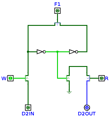
The following diagram shows the same circuit but with the inverters replaced with the inverter symbol (and I've also split D2 into D2IN and D2OUT, because Logisim doesn't seem to support a dual purpose input/output):
control_register_cell_logisim.png
control_register_cell_logisim.png (3 KiB) Viewed 5787 times
The design is similar to a couple of circuits that are discussed in the Mead/Conway "Introduction to VLSI Systems" book that I've referred to previously:

http://ai.eecs.umich.edu/people/conway/ ... -sided.pdf

From chapter 3, Fig 8:
register_cell_mead_conway_sect3_fig8.png
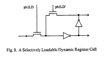
register_cell_mead_conway_sect3_fig8.png (14.53 KiB) Viewed 5787 times
And from chapter 5, Fig 22:
register_cell_carver_mead_chap5_fig22.png
(although the above diagram shows the inverters in their transistor form rather than logical symbol)

Figure 22 is interesting because it shows a dual port register, which means that its value can be set and read from two different data bus lines. Let's ignore that though, because the 6561 only has one data bus for reading and writing. This is what makes Figure 22 relevant though, because if we ignore the second bus and focus on only one bus, then the diagram looks like this:
register_cell_carver_mead_chap5_fig22_one_bus.png
It appears to show the data in and data out sharing the same bus line. Later on in the same chapter (chapter 5), it shows the silicon layout (figure 22a) for the dual port register cell and it is clear that, yes, the same data line is shared for both input and output. This is relevant because in the case of the 6561, the same data line is used for both input to the register cell and output from it. The above diagram is close to what I showed in the first logisim diagram for the 6561 register cell. The obvious difference is with regards to the way that the reading is done. I've looked at this part of the die shot many times and I always come up with the same schematic. Rather than taking the output value from the point after the two inverters and connecting that directly to the data line, it instead takes the value from the point between the two inverters (so is the inverted value stored in the register cell) and then connects that value up to the gate of a pull down transistor. The drain side of that transistor is then connected to the "R"ead pass transistor. So if the point between the two inverters is HIGH (which represents the register cell storing a zero), then it pulls the data line LOW when the R pass transistor is turned on.

As I discussed in that post from the older thread, this seems to make sense only if there is a pull up somewhere along the data line that is active when data is being read from a control register. I haven't yet found such a pull up, but it feels like it should be there somewhere, otherwise the above circuit (i.e. the first one drawn in logisim) has a way of pulling the data line LOW on Read, but when the register cell is in the other state, there would be nothing pulling the data line HIGH.

Chapter 3 of the Mead/Conway book has an interesting discussion about how the charge is stored within the register cell, or more generically, how it is isolated on the input gate of an inverter's pull down transistor (the shift register sections goes into a bit of detail regarding this). Applying this to the 6561 register cell, when the data line is HIGH and W is high, then the gate capacitance of the first inverter's input is charged up. When W goes LOW, the charge is isolated on that transistor gate, and due to the feedback path through the F1 controlled pass transistor, it holds that charge indefinitely. Now when the data line is LOW, and W goes HIGH, it is designed to be HIGH at least long enough for the charge on the first inverter's input gate to discharge, which sets the register cell to be zero/low. When W goes LOW, that "lack of charge" is isolated there.
Kakemoms
Vic 20 Nerd
Posts: 740
Joined: Sun Feb 15, 2015 8:45 am

Re: 6561 Die Shot Reversing Explorations

Post by Kakemoms »

Ok. Thank you for the long explanation. I didn't understand that the double circles were Vcc in the first diagram (maybe I was too sleepy), and with OUT at the top instead of the bottom, it made less sense.

With the modified diagram it makes perfectly sense. :D
Jogi
Pinballer
Posts: 84
Joined: Thu Jan 12, 2006 2:30 am
Website: http://www.vic20.de
Location: Germany

Re: 6561 Die Shot Reversing Explorations

Post by Jogi »

Hi,

DIE Shot 6561-101

[attachment=0]6561R0.JPG[/attachment

https://www.forum64.de/index.php?thread ... ous-video/

Regards Jogi
Attachments
6561R0.JPG
lance.ewing
Vic 20 Afficionado
Posts: 413
Joined: Sat Nov 10, 2012 3:19 pm
Website: https://sites.google.com/site/mos6561vic/

Re: 6561 Die Shot Reversing Explorations

Post by lance.ewing »

Hey, this is great! Thank you very much. I shall take a close look this evening.
lance.ewing
Vic 20 Afficionado
Posts: 413
Joined: Sat Nov 10, 2012 3:19 pm
Website: https://sites.google.com/site/mos6561vic/

Re: 6561 Die Shot Reversing Explorations

Post by lance.ewing »

Jogi wrote:DIE Shot 6561-101
Do you have access to the full size image? Although I recognise the chip, and am very familiar with the patterns and shapes seen in this image, it isn't close enough to make out any detail or differences with the 6561E.
lance.ewing
Vic 20 Afficionado
Posts: 413
Joined: Sat Nov 10, 2012 3:19 pm
Website: https://sites.google.com/site/mos6561vic/

Re: 6561 Die Shot Reversing Explorations

Post by lance.ewing »

Even at this resolution, I can tell that the 4 sine/cosine generators for the chrominance are a different layout, and also the logic to the side of this, including the Phase Alternating logic and sub-carrier drivers. They're a different layout as well. The layout for the resistors that control the mixing of the two chosen sine/cosine wave forms for the chrominance is also a different layout.

It looks like the POT comparator layout is also different, including the metal layer being quite different.

Edit: It is a bit different down by the option pads as well. The light pen pad and the layout of the initial logic (diffusion and polysilicon) that the signal goes through is different.
Post Reply