Introducing VFLI for VIC-20: 208x256 pixels in 16 colours!

Modding and Technical Issues

Moderator: Moderators

Post Reply
User avatar
Mike
Herr VC
Posts: 4833
Joined: Wed Dec 01, 2004 1:57 pm
Location: Munich, Germany
Occupation: electrical engineer

Part 3: Finale - replacing UE1 for more colours

Post by Mike »

Expanding the internal RAM from 5K to 8K already allows to display the 208x256 pixels mode of MAXIGRAFIK without any significant CPU usage. This frees up the 6502 for other tasks. It now can, for example, provide independent background/border and auxiliary colour on every raster. And FLI over the whole screen width is made possible by replacing UE1 with a chip of 16 times the capacity. Its 16 "banks" are switched on every raster, too - leading to 8x1 attribute cells!

Here are the pinouts of 2114 and CY7C164 in comparison:

Code: Select all

                              CY-7C164
                            +----\/----+
        2114             1 -|A5     Vcc|- 22
    +----\/----+         2 -|A6      A4|- 21
 1 -|A6     Vcc|- 18     3 -|A7      A3|- 20
 2 -|A5      A7|- 17     4 -|A8      A2|- 19
 3 -|A4      A8|- 16     5 -|A9      A1|- 18
 4 -|A3      A9|- 15     6 -|A10     A0|- 17
 5 -|A0    I/O1|- 14     7 -|A11   I/O3|- 16
 6 -|A1    I/O2|- 13     8 -|A12   I/O2|- 15
 7 -|A2    I/O3|- 12     9 -|A13   I/O1|- 14
 8 -|/CS   I/O4|- 11    10 -|/CE   I/O0|- 13
 9 -|GND    /WE|- 10    11 -|GND    /WE|- 12
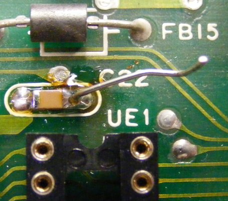
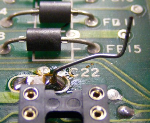
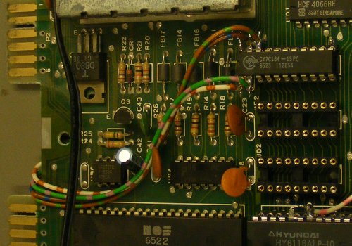
    +----------+            +----------+
With the exception of 5 pins of the CY7C164, all others have a comparable function: /WE, /CE, GND, and most data and address pins are at the same place. For a SRAM chip it doesn't matter that the address and data pins are permuted in within their respective groups. Reading data back reverses any permutation in that case (this would not be true for EPROMs).

Pins 1, 2, 20, 21, and 22 of the CY7C164 need special treatment however. They're bent straight like done with UC4 and U13. To provide Vcc to pin 22, C22 on the mainboard needs to be desoldered, and a SMD capacitor of 100 nF and a solid wire on the +5 V side be soldered instead, so the wire can reach to the straightened pin 22:

Image Image

Now solder long braided wires to the pins 1, 2, 20, and 21 of the chip. These are the new address lines connected to the userport, as follows:

Code: Select all

Pin 1  <-> userport connector F (designated colour RAM address A13, brown-white wire on photos)
Pin 2  <-> userport connector E (new A12, pink-green)
Pin 21 <-> userport connector D (new A11, blue-brown)
Pin 20 <-> userport connector C (new A10, green-brown)
When the chip is inserted, with its bottom edge aligned to the bottom edge of the socket, solder pin 22 to the solid wire. That should look like this:

Image

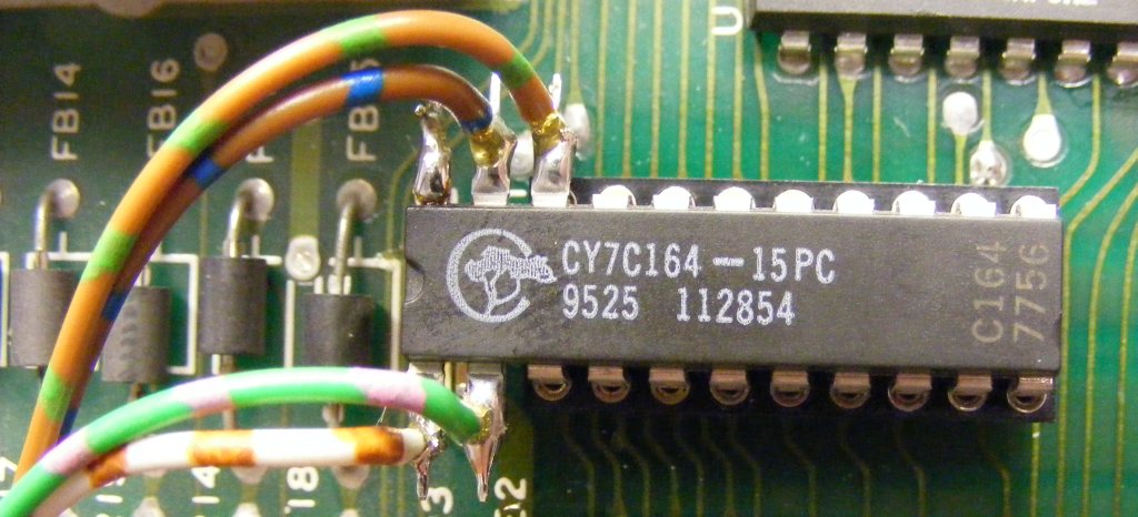
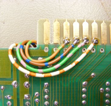
The wires are guided to the right side of the userport (viewed with the userport facing away) and then soldered to the bottom end of the board connector row, on the soldering side of the mainboard, pins C to F:

Image Image

Congratulations! You're done. :D

The lower four bits of VIA1 port B (address $9110, decimal: 37136) now control the FLI bank. As long as the DDR register ($9112) is not initialised to 15, internal pull-ups in the NMOS variant of the VIA select bank 15 of the colour RAM. The banking is activated with POKE 37138,15. The bank then is selected with POKE 37136,x (x=0..15). Two *.d64 images with 15 images each in VFLI mode will follow shortly for you to try out the new hardware. :)
Last edited by Mike on Sun Jun 29, 2014 1:59 pm, edited 2 times in total.
User avatar
Mike
Herr VC
Posts: 4833
Joined: Wed Dec 01, 2004 1:57 pm
Location: Munich, Germany
Occupation: electrical engineer

Post by Mike »

So, here's vfli.zip (download). Below is another one of the 30 pictures stored in the two *.d64 image files:

Image

The viewer requires a PAL VIC-20 with above VFLI mod and an external 8K RAM expansion.

Source code of the display routine and a description of the VFLI file format have been included as well.

Greetings,

Michael
Last edited by Mike on Thu Feb 20, 2014 4:16 pm, edited 2 times in total.
User avatar
e5frog
Vic 20 Nerd
Posts: 551
Joined: Sat Feb 17, 2007 5:46 pm
Website: http://channelf.se
Location: Sweden
Occupation: Service Engineer

Post by e5frog »

How long does it take to load and display the picture?
My other interest: http://channelf.se
User avatar
Mike
Herr VC
Posts: 4833
Joined: Wed Dec 01, 2004 1:57 pm
Location: Munich, Germany
Occupation: electrical engineer

Post by Mike »

e5frog wrote:How long does it take to load and display the picture?
The file size is 10499 bytes including the 2-byte load address, i.e. 42 blocks.

The files are loaded with the standard LOAD kernal vector call, in one piece. Without fast loader, this takes maybe half a minute. On my FE3 with SJLOAD, only 3-4 seconds.
Last edited by Mike on Fri May 10, 2013 3:25 pm, edited 1 time in total.
User avatar
Ghislain
Realms of Quest
Posts: 1279
Joined: Sun Aug 08, 2004 12:54 am

Post by Ghislain »

Impressive. I remember soldering being my least favorite part of my classes in college (I burned myself many many times). I haven't touched a soldering iron in years, I think I would fry my VIC-20 if I dared to try this. I was all thumbs with even a dummy breadboard. I can't imagine even desoldering chips from a real Commodore board.

I have a silly question though.

Why is normal 3K cartridge memory expansion from 0400-0FFF inadequate for 208x256 VLFI mode?

(I'm certain that there's a valid technical reason of course)

As well, is this newly-modified VIC-20 backwards compatible?
"A slave is one who waits for someone to come and free him." -- Ezra Pound
User avatar
Ghislain
Realms of Quest
Posts: 1279
Joined: Sun Aug 08, 2004 12:54 am

Post by Ghislain »

Ghislain wrote:Impressive. I remember soldering being my least favorite part of my classes in college (I burned myself many many times). I haven't touched a soldering iron in years, I think I would fry my VIC-20 if I dared to try this. I was all thumbs with even a dummy breadboard. I can't imagine even desoldering chips from a real Commodore board.

I have a silly question though.

Why is normal 3K cartridge memory expansion from 0400-0FFF inadequate for 208x256 VLFI mode?

(I'm certain that there's a valid technical reason of course)

As well, is this newly-modified VIC-20 backwards compatible?
I guess the most obvious answer must be that the VIC chip (or the internal VIC-20 hardware that communicates with it) differentiates between internal "natural" ram and external "cartridge" ram? I never tested this myself. I always assumed that the VIC-20 graphics chips were able to "see" whatever was in memory locations 0000-1FFF.

I think it would have been pretty cool if the VIC-20 always had 8K of internal RAM right from the get-go.
"A slave is one who waits for someone to come and free him." -- Ezra Pound
User avatar
Mike
Herr VC
Posts: 4833
Joined: Wed Dec 01, 2004 1:57 pm
Location: Munich, Germany
Occupation: electrical engineer

Post by Mike »

Ghislain wrote:I guess the most obvious answer must be that the VIC chip (or the internal VIC-20 hardware that communicates with it) differentiates between internal "natural" ram and external "cartridge" ram?
Exactly.
As well, is this newly-modified VIC-20 backwards compatible?
It's still possible to temporarily 'unexpand' the VIC-20 by issuing 'POKE642,16:POKE644,30:POKE648,30:SYS64818'. When there is a game cartridge inserted, that method obviously is not applicable. Even though, screen and colour RAM are still at the same addresses like on an unexpanded VIC, so cartridges relying on fixed addresses in that range are still supposed to work.

The colour RAM banking takes four address bits from the userport. For the moment, this precludes the usage of the userport for RS232.
User avatar
Mike
Herr VC
Posts: 4833
Joined: Wed Dec 01, 2004 1:57 pm
Location: Munich, Germany
Occupation: electrical engineer

Post by Mike »

Here's '3k.prg' (download). Just load it ',8,1' to unexpand the VIC-20 - that should be a little easier than remembering the above incantation. ;)

It's only 30 bytes in size, and I've put it in the root directory of my SD card.
Last edited by Mike on Thu Feb 20, 2014 4:16 pm, edited 2 times in total.
Kananga
Vic 20 Afficionado
Posts: 317
Joined: Mon Mar 08, 2010 2:11 pm

Post by Kananga »

Is it possible to detect your expansion from software?
I thought about how to detect the 3K being accessible from the VIC, but that's perhaps a task for tlr.
I would adopt the vic GUI to use the extra 3K for video ram and offer 26 character blocks in addtion (for PAL), but I'd like to have no dedicated binary. Right now, all different configurations (RAM, PAL, NTSC) are covered by one binary.
Buy the new Bug-Wizard, the first 100 bugs are free!
User avatar
Mike
Herr VC
Posts: 4833
Joined: Wed Dec 01, 2004 1:57 pm
Location: Munich, Germany
Occupation: electrical engineer

Post by Mike »

Kananga wrote:Is it possible to detect your expansion from software?
I thought about how to detect the 3K being accessible from the VIC, but that's perhaps a task for tlr.
That should be possible by putting screen and char data into the range of $0400 of $0FFF (after the presence of the 3K itself has been established), these forming an easy to find signature string when read out over unconnected memory. An external 3K expansion would not be able to reproduce that string. Much the same method tlr uses in his 'timing.prg', indeed.
I would adopt the vic GUI to use the extra 3K for video ram and offer 26 character blocks in addition (for PAL), but I'd like to have no dedicated binary.
Me :D!

I'm also working on light-weight version of the graphics mode, where 208x256 without FLI (i.e. like MAXIGRAFIK, but now with ~100% available CPU for the user program) is realised with just 3 raster splits of NMI. In that case, vin could do a simple bitmap access from $0600 to $1FFF. I'll just have to check, if that method plays nice with disc access. ;)
User avatar
Mike
Herr VC
Posts: 4833
Joined: Wed Dec 01, 2004 1:57 pm
Location: Munich, Germany
Occupation: electrical engineer

Post by Mike »

Here's a working prototype of the detection routine: (download). Besides the 3K expansion it also needs at least an external 8K expansion. Source is included. Since I couldn't test it on my unmodded VIC-20, it should also be interesting to run it on an unmodded VIC-20, to make sure it doesn't return false positives. Both PAL and NTSC are supported.

...

During that session, I also wrote 'max.prg' (download, load with ',8,1'), which moves screen memory down to $0400 and the BASIC start to $0601, providing up to 31231 BYTES FREE for BASIC with a +24K RAM expansion. :mrgreen:

Cheers,

Michael
Last edited by Mike on Thu Feb 20, 2014 4:17 pm, edited 2 times in total.
Kananga
Vic 20 Afficionado
Posts: 317
Joined: Mon Mar 08, 2010 2:11 pm

Post by Kananga »

Mike wrote:Here's a working prototype of the detection routine: (download). Besides the 3K expansion it also needs at least an external 8K expansion. Source is included. Since I couldn't test it on my unmodded VIC-20, it should also be interesting to run it on an unmodded VIC-20, to make sure it doesn't return false positives. Both PAL and NTSC are supported.
Great, thanks! And here I was already trying to figure out how to do it... I will give it a try at the weekend. Too much work presently :(
Buy the new Bug-Wizard, the first 100 bugs are free!
User avatar
GreyGhost
Vic 20 Nerd
Posts: 525
Joined: Wed Oct 05, 2005 11:10 pm

Post by GreyGhost »

Heck Mike, why not move it down a little further ($0338) and grab the cassette buffer too. :D
Rob
User avatar
tokra
Vic 20 Scientist
Posts: 1123
Joined: Tue Apr 27, 2010 5:32 pm
Location: Scheessel, Germany

Post by tokra »

Display memory can only be placed at $0200-byte steps, so $0338 is not possible. However you can gain a whopping 6 bytes, by placing the BASIC-start $05fa instead of $0600.
User avatar
GreyGhost
Vic 20 Nerd
Posts: 525
Joined: Wed Oct 05, 2005 11:10 pm

Post by GreyGhost »

Ah crap. I knew that. I was thinking about the 3k expansion and screen memory being where it is for unexpanded vic ($1e00)and moving basic up to $0338. My bad.
Rob
Post Reply