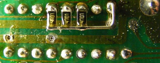
Expanding the internal RAM from 5K to 8K already allows to display the 208x256 pixels mode of MAXIGRAFIK without any significant CPU usage. This frees up the 6502 for other tasks. It now can, for example, provide independent background/border and auxiliary colour on every raster. And FLI over the whole screen width is made possible by replacing UE1 with a chip of 16 times the capacity. Its 16 "banks" are switched on every raster, too - leading to 8x1 attribute cells!
Here are the pinouts of 2114 and CY7C164 in comparison:
Code: Select all
                              CY-7C164
                            +----\/----+
        2114             1 -|A5     Vcc|- 22
    +----\/----+         2 -|A6      A4|- 21
 1 -|A6     Vcc|- 18     3 -|A7      A3|- 20
 2 -|A5      A7|- 17     4 -|A8      A2|- 19
 3 -|A4      A8|- 16     5 -|A9      A1|- 18
 4 -|A3      A9|- 15     6 -|A10     A0|- 17
 5 -|A0    I/O1|- 14     7 -|A11   I/O3|- 16
 6 -|A1    I/O2|- 13     8 -|A12   I/O2|- 15
 7 -|A2    I/O3|- 12     9 -|A13   I/O1|- 14
 8 -|/CS   I/O4|- 11    10 -|/CE   I/O0|- 13
 9 -|GND    /WE|- 10    11 -|GND    /WE|- 12
    +----------+            +----------+
With the exception of 5 pins of the CY7C164, all others have a comparable function: /WE, /CE, GND, and most data and address pins are at the same place. For a SRAM chip it doesn't matter that the address and data pins are permuted in within their respective groups. Reading data back reverses any permutation in that case (this would not be true for EPROMs).
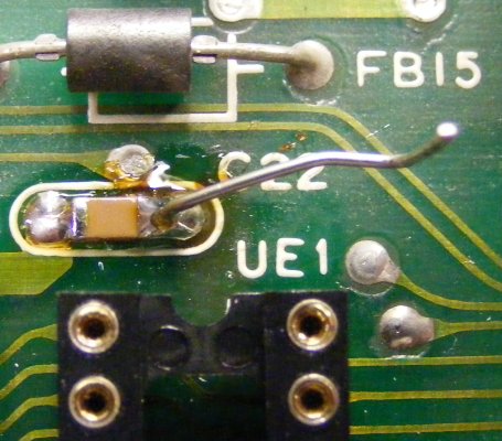
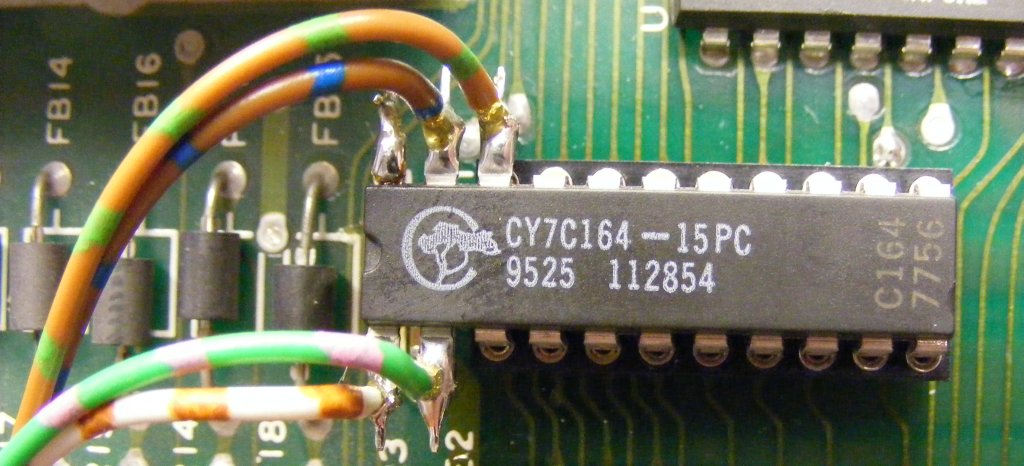
Pins 1, 2, 20, 21, and 22 of the CY7C164 need special treatment however. They're bent straight like done with UC4 and U13. To provide Vcc to pin 22, C22 on the mainboard needs to be desoldered, and a SMD capacitor of 100 nF and a solid wire on the +5 V side be soldered instead, so the wire can reach to the straightened pin 22:
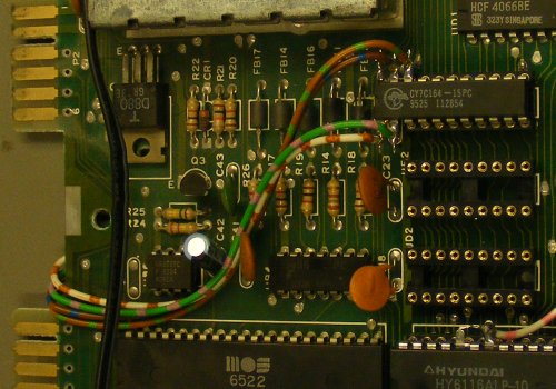
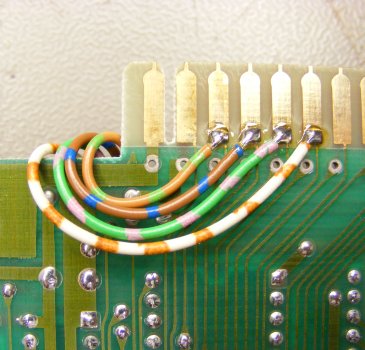
Now solder long braided wires to the pins 1, 2, 20, and 21 of the chip. These are the new address lines connected to the userport, as follows:
Code: Select all
Pin 1  <-> userport connector F (designated colour RAM address A13, brown-white wire on photos)
Pin 2  <-> userport connector E (new A12, pink-green)
Pin 21 <-> userport connector D (new A11, blue-brown)
Pin 20 <-> userport connector C (new A10, green-brown)
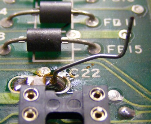
When the chip is inserted, with its bottom edge aligned to the bottom edge of the socket, solder pin 22 to the solid wire. That should look like this:
The wires are guided to the right side of the userport (viewed with the userport facing away) and then soldered to the bottom end of the board connector row, on the soldering side of the mainboard, pins C to F:
Congratulations! You're done.

The lower four bits of VIA1 port B (address $9110, decimal: 37136) now control the FLI bank. As long as the DDR register ($9112) is not initialised to 15, internal pull-ups in the NMOS variant of the VIA select bank 15 of the colour RAM. The banking is activated with
POKE 37138,15. The bank then is selected with
POKE 37136,x (x=0..15). Two *.d64 images with 15 images each in VFLI mode will follow shortly for you to try out the new hardware.