Ram Expander

Modding and Technical Issues

Moderator: Moderators

User avatar
amramsey
Vic 20 Hobbyist
Posts: 117
Joined: Sat Apr 14, 2007 9:38 pm

Ram Expander

Post by amramsey »

Well, after re-discovering my Vic and all the fun that can be had with it, I've come to the realization that I need a ram expander. Now, I could go and buy one but what would be the fun in that? :D I've been scouring the forums getting familiar with how the expansion bus works. Man, why the heck didn't Commodore just drive all the address lines out to the port and let the cartridges do the decoding? :P

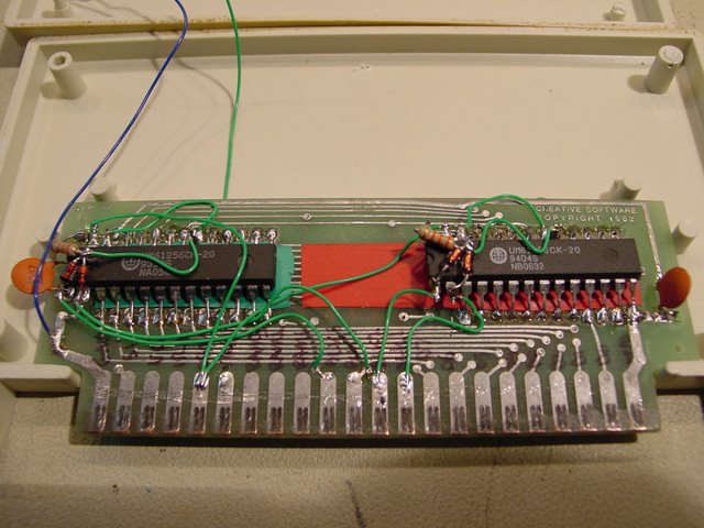
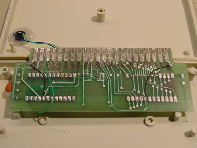
Once I decided that I was going to build a ram cartridge, I figured that I might as well make one that has ram in every hole that the vic has... BLK1-3,5 and RAM1-3. Now, that takes either four chips (32k + 3 1k chips) or 2 chips (32k + 8k) or 1 chip (64k). 1 chip is the obvious choice, but all that wasted ram just irked me. :lol: It seems natural to make some use of it, so why not set up BLK5 so it can be bank-switched for the heck of it?

A quick scan of Digikey for ram chips turned up no 5V 64k ram chips in stock, but a nice looking 128k ram chip (CY62128E). Being as I was already bank switching, why not switch a little more? :lol: You can see where this is going.

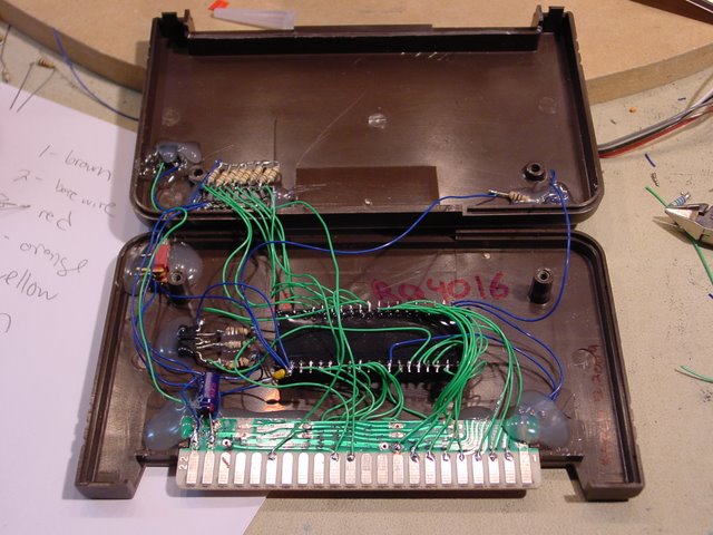
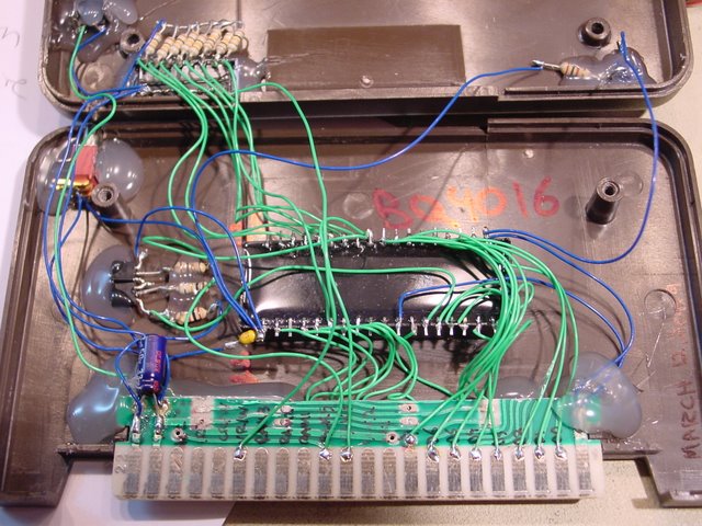
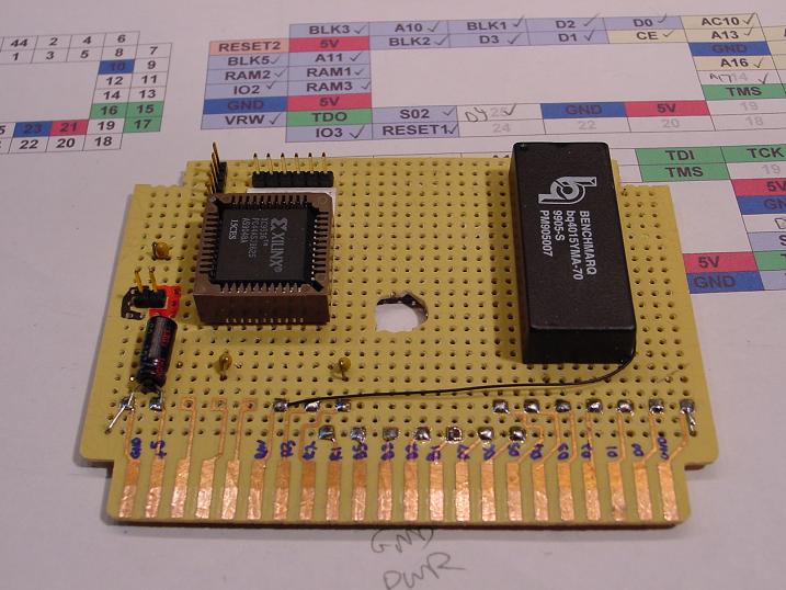
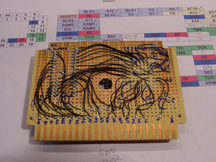
Anyhow, so my plan is to wire together a small board with a CPLD and the ram chip. I'm using a simply XL9500 CPLD to reduce the number of logic chips, and also because I've got them kicking around and not many discrete logic chips. :wink:

So the basic idea is to make the 3 1k blocks into the first 8k of SRAM, BLK1-3 into the next 8k blocks and then let BLK5 use the last 12 blocks of 8k ram. I'll latch the data lines D0-D3 and use them to provide address decoding for the BLK5 blocks. That would be latched during a write access into I02.

Memory map:

Code: Select all

                                        SRAM Addr.    Vic Addr.  Notes
      A10 A11  A13   A14   A15   A16    Low    High   Low   High   
RAM1   1   0    0     0     0     0    $00400 $007FF $0400 $07FF   
RAM2   0   1    0     0     0     0    $00800 $00BFF $0800 $0BFF   
RAM3   1   1    0     0     0     0    $00C00 $00FFF $0C00 $0FFF   
BLK1   -   -    1     0     0     0    $02000 $03FFF $2000 $3FFF   
BLK2   -   -    0     1     0     0    $04000 $05FFF $4000 $5FFF   
BLK3   -   -    1     1     0     0    $06000 $07FFF $6000 $7FFF   
BLK5   -   -   D0=0  D1=0  D2=1  D3=0  $08000 $09FFF $A000 $BFFF PAGE 0
BLK5   -   -   D0=1  D1=0  D2=1  D3=0  $0A000 $0BFFF $A000 $BFFF PAGE 1
BLK5   -   -   D0=0  D1=1  D2=1  D3=0  $0C000 $0DFFF $A000 $BFFF PAGE 2
BLK5   -   -   D0=1  D1=1  D2=1  D3=0  $0E000 $0FFFF $A000 $BFFF PAGE 3
BLK5   -   -   D0=0  D1=0  D2=0  D3=1  $10000 $11FFF $A000 $BFFF PAGE 4
BLK5   -   -   D0=1  D1=0  D2=0  D3=1  $12000 $13FFF $A000 $BFFF PAGE 5
BLK5   -   -   D0=0  D1=1  D2=0  D3=1  $14000 $15FFF $A000 $BFFF PAGE 6
BLK5   -   -   D0=1  D1=1  D2=0  D3=1  $16000 $163FF $A000 $BFFF PAGE 7
BLK5   -   -   D0=0  D1=0  D2=1  D3=1  $18000 $19FFF $A000 $BFFF PAGE 8
BLK5   -   -   D0=1  D1=0  D2=1  D3=1  $1A000 $1BFFF $A000 $BFFF PAGE 9
BLK5   -   -   D0=0  D1=1  D2=1  D3=1  $1C000 $1DFFF $A000 $BFFF PAGE 10
BLK5   -   -   D0=1  D1=1  D2=1  D3=1  $1E000 $1FFFF $A000 $BFFF PAGE 11


I banged together some quick verilog. I must have done something wrong because it ended up being easier than I though and I'm only using about a third of a XL9532 CPLD (basically the smallest one that can be found). :lol: I'm going to wire together something this weekend to see if it works. I couldn't get the damn xilinx simulator to simulate my code (its been years since I did anything with programmable logic) so I'll just have to program the CPLD and see what happens. :shock:

I wasn't 100% sure of the vic-20 bus timing though. When should I be latching data lines? I'm going to have to hook my logic analyzer up to the bus to see exactly, but it looked like data lines can be latched on the rising edge of I02? If not, I'll have to latch on the S02 clock line instead. Figured I'd keep it simple for the time being.

Once I get this running, my next step will be to interface a small pic controller and an SD flash card into it. I've done all the code for reading from an sdcard from previous projects. On the face of it, it looks pretty easy to make a generic flash cart for the vic. Basically the PIC processor would hold the VIC in reset, read a bootmenu program from the SD card and put it into BLK5 of the RAM as well as read the directory listing from the SD card and dump that also into RAM. When the VIC comes out of reset, it runs the program and lets the user select what they want to run from the flash card. When the user has selected, that triggers the PIC to reset the PIC, load the program into RAM and then passes control back to the PIC.

Anyhow, anyone see any issues with my planned implementation of a ram cart? Is there a standard for bank switching on the vic that I should be following?
Unseen
Vic 20 Amateur
Posts: 47
Joined: Sun Feb 01, 2009 9:16 am

Re: Ram Expander

Post by Unseen »

amramsey wrote:Basically the PIC processor would hold the VIC in reset, read a bootmenu program from the SD card and put it into BLK5 of the RAM
Have you found any documentation about the 6502 behaviour during reset?

I know that the NMOS versions can be halted using RDY during execution, but in that case the address lines are not tristated. It would be interesting if they are while the chip is held in reset.
User avatar
amramsey
Vic 20 Hobbyist
Posts: 117
Joined: Sat Apr 14, 2007 9:38 pm

Post by amramsey »

Ah, that's interesting. My assumption is that the 6502 would play nice and tristate the lines. I'll have to take a closer look. Worst case would be tristate buffers everywhere to make sure that everyone is happy. :x
Leeeeee
soldering master
Posts: 396
Joined: Fri Apr 23, 2004 8:14 am

Post by Leeeeee »

My assumption is that the 6502 would play nice and tristate the lines.
Bwaaaaaaaahahahahahahaha.

No it doesn't play nice.

If the CPLD/PIC/whatever you want to drive the RAM can tristate its own lines then one method that works is to put series resistors of a few hundred ohms between the 6502 and the RAM. In normal operation the RAM is easily driven via these resistors and when the 6502 is halted the CPLD/PIC/whatever drives the RAM end of the resistors overcomming the 6502's drive.

No resistors are used on the data bus lines as the 6502 can only be halted during a read cycle so those lines will be inputs and thus not driving the lines.

Lee.
User avatar
amramsey
Vic 20 Hobbyist
Posts: 117
Joined: Sat Apr 14, 2007 9:38 pm

Post by amramsey »

Dang! Not only am I building hardware for an outdated computer, Xilinx went and dropped support for the CPLDs that I have kicking around in the my lab! Arg! I've been messing with the hardware today and couldn't get the CPLD programmed. The programming tools were seeing it but wouldn't let me go any further. I'm working with a laptop that I hadn't done this type of stuff before, along with a dusty old parallel port JTAG programmer that I haven't touched in about 6 years.... My natural inclination was that something was funky with either the laptop or the programmer. :evil: Turns out Xilinx dropped programming support for this chip a few year back.... but left the ability to still choose that chip when compiling verilog code!!?!! :x

Dug thru my software and found some seriously old Xilinx software to go along with my seriously old CPLDs and PC. Installing it now. Retro development at its best. No doubt I'll be soon installing windows 95 somewhere to make it all work. :lol:

And I thought that using programmable logic would save me time! :wink:
User avatar
nbla000
Salmon Run
Posts: 2582
Joined: Thu Oct 13, 2005 8:58 am
Location: Italy

Re: Ram Expander

Post by nbla000 »

amramsey wrote:Well, after re-discovering my Vic and all the fun that can be had with it, I've come to the realization that I need a ram expander.
Talking about RAM expansion, the Mega-Cart gives your vic-life very easy, take a look to the memory expander section for further info.
Mega-Cart: the cartridge you plug in once and for all.
User avatar
amramsey
Vic 20 Hobbyist
Posts: 117
Joined: Sat Apr 14, 2007 9:38 pm

Re: Ram Expander

Post by amramsey »

nbla000 wrote:
amramsey wrote:Talking about RAM expansion, the Mega-Cart gives your vic-life very easy, take a look to the memory expander section for further info.
Sure, but what would be the fun in that? :D
User avatar
amramsey
Vic 20 Hobbyist
Posts: 117
Joined: Sat Apr 14, 2007 9:38 pm

Post by amramsey »

Leeeeeeeee eee eeeeeee scared me a bit and I figured that I'd better scale back a bit on my first board for the Vic. I dug through my cart collection last weekend and found two carts with full edge connectors on them... and happily both of them were pretty crappy games. :D

First I decided that I wanted to play some of the games, so I'd build a simple BLK5 cart with a dip switch to switch between different games. I've got a bunch of BQ4016s kicking around on my shelf that I sampled for free a few years back so I figured that this would make a nice start. The BQ4016 is a 1Mx8 RAM module with a battery backup that lasts around 10 years. I'll have something better by then so the battery life didn't scare me off. I hacked off everything from the cart PCB except for the header and point-to-point wired it all up... using lots of hot glue to keep it all together. :D

After building it, I realized that there were some cool BLK3/BLK5 games that I wanted to play also... so I tore it back open, ANDed the BLK3 and BLK5 together using transistors and drove BLK3 into one of the address lines to give me a 16k cart (with 64 games). Sure... a bunch of the memory is wasted when I'm loading 8k games. Ah well....

Image
Image
Image

So I plugged it in the Vic-20, wrote a quick program to test the memory and then.... damn! No way to get games onto it.
:lol: So I built a 64HDD machine with a 512Meg flash drive to load the games and what not from. (Details in another thread).

Life was good for a few days, until I discovered that there were yet more games that I couldn't play... like Temple of Apshai or Sword of Fargoal. Some other games like Cannonball Blitz used different memory blocks even.

So, back to the drawing board. I looked in the other cart that I had with a full edge connector and it had space for two roms. The pinout of those roms was similar to some old computer cache memory that I had sitting around, aside from the cache memory being 2 pins longer and narrow instead of wide. A little bending later, a couple cut tracks and a couple of AND gates built from diodes and I had a 32k ram cart. :D

Image
Image
Image

Played with it a bit tonite.... Sword of Fargoal kicked my butt. :lol: On the other hand, DigDug is ridiculously easy. Same goes for Galaxian... the difficultly just never seems to ramp up.

Maybe I'm just used to getting my *ss handed to me in Omega Race. :x

I just got some prototyping board in the mail today (thanks ArcadeComponents!!) so I'm ready to move onto bigger boards with the CPLD. My verilog code for the bank-switched FPGA seems to be simulating ok and I finally found a very old version of the Xilinx tools that will program my stupidly old CPLDs so I should be ready to roll. With a couple more games on the side....
:lol:
gklinger
Vic 20 Elite
Posts: 2051
Joined: Tue Oct 03, 2006 1:39 am

Post by gklinger »

Nice work. You even made fancy labels.

I'm reminded of this.
In the end it will be as if nothing ever happened.
User avatar
amramsey
Vic 20 Hobbyist
Posts: 117
Joined: Sat Apr 14, 2007 9:38 pm

Post by amramsey »

gklinger wrote:Nice work. You even made fancy labels.
The carts were looking pretty ugly without them (not that they are very pretty with them... :lol: ) The ones the Hawk did are much nicer. I figured that I didn't have the skill to emulate the true C= design so I'd head in the other direction.
gklinger wrote:I'm reminded of this.


I ordered samples of that nvram device the 6502dude found but haven't received them yet. I may have to break down and actually buy a few at some point. I think that it would be better to have two of the chips piggybacked though to give a 16k cart, with the blocks being switchable in location to cover more of the 16k roms.
User avatar
amramsey
Vic 20 Hobbyist
Posts: 117
Joined: Sat Apr 14, 2007 9:38 pm

Post by amramsey »

Its ALIVE! :D I now have a functional 512kbyte Vic-20.

All my CPLD code actually worked first time..... well.... mostly. :lol: Originally I was latching my bank values in on the rising edge of IO2 and ignoring RW... everything would work ok for a few hundred milliseconds and then a random event would wipe out my latched values. I didn't go digging around much on the logic analyzer to find out what it was... instead switched over to latching the data values in on the rising edge of RW instead.

I went bananas yesterday when I first wired the board up.... I was getting strange errors in certain areas of my ram... I thought I was having timing errors with my CPLD and kept scaling the code back until the CPLD was basically doing nothing and it was still failing. Checked all my solder connections and everything was looking ok. I finally started checking right from the pins of the card back and found that the copper on a trace running from the pin for address 8 was cracked! I didn't pop it under the microscope to take a close look but there must have been a hairline crack in the old copper on my seriously old prototyping boards. :evil: You can see the extra solder I ran on that trace on the second picture.

Once I sorted that out, it was all clear sailing.

It takes roughly an hour for basic to poke a 0 to every location in my bankswitched card. Ouch! There are 60 banks of 8k each sitting at $A000 (BLK5). They are switched by poking to any address in IO2 memory space ($9800 or 38912 decimal). The first 4 blocks overlap my RAM1/2/3 and BLK1/2/3 spaces in order to make the implementation in the CPLD nice and easy.

I didn't have any big ram chips sitting around so I used a 512k battery back ram module from TI (BQ4015). It would be trivial to extend this to 2048k of ram (still have pins left on the CPLD) but I'm not sure what the point would be. :D Not that there is any point to a 512k Vic anyhow. :lol:

So I did up the schematics and a PCB design for this board also. Looks like PCBs would be about $5 + around $10 for the CPLD and ramchip (128k) in small quantities. Based on the lack of interest in a bank-switch ram cart though, I think that I'll chalk this one up as a fun experiment and move on to a SD flash cart for the Vic instead. :D

Image
Image

No pretty cover for it yet. It fits in a normal Commodore cartridge.

Video showing a little program switching through the banks:
http://www.youtube.com/watch?v=1d5bJSGCqlM

And to show how easy the Verilog code for the CPLD is:

Code: Select all

module top(ram1, ram2, ram3, blk1, blk2, blk3, blk5, io2, io3, a10i, a11i, a10o, a11o, a13o, a14o, a15o, a16o, a17o, a18o, di , rw, s02clk, cs, reset, debug0, debug1, debug2, debug3, debug4);
    input ram1;
    input ram2;
    input ram3;
    input blk1;
    input blk2;
    input blk3;
    input blk5;
	 input io2;      
	 input io3;      
    input a10i;     // address line 10 input - controlled by ram1..3
    input a11i;     // address line 11 input - controlled by ram1..3
    output a10o;    // address line 10 output
    output a11o;    // address line 11 output
    output a13o;    // address line 13 output
    output a14o;    // address line 14 output
    output a15o;    // address line 15 output
    output a16o;    // address line 16 output
    output a17o;    // address line 17 output
    output a18o;    // address line 18 output
    input [5:0] di; // data line inputs, used to set blk5 bank number
    input rw;       // read/write from vic20 if needed
    input s02clk;   // clock input if needed to clock in data (likely not necessary)
	 output cs;      // chip select generated from ram1/ram2/ram3/blk1/blk2/blk3/blk5
    input reset;    // in case we need a reset at the start
    output debug0;
    output debug1;
    output debug2;
    output debug3;
    output debug4;
//*******************************************************************
// various registers that I might need
//*******************************************************************
reg [5:0] bank; // BLK5 bank number that user has selected

//*******************************************************************
//*******************************************************************
assign cs=blk1&blk2&blk3&blk5&ram1&ram2&ram3; // any of them low causes CS to go low
// if all of the ram lines are high, output a10i to a10o, otherwise....
//   if ram2 is low, output low on A10 and if ram2 is high, output high on this line
assign a10o=(ram1&ram2&ram3)?a10i:(ram2?1'b1:1'b0);
// if all of the ram lines are high, output a11i to a11o, otherwise...
//   if ram1 is low, output low on A11 and if ram1 is high, output high on this line
assign a11o=(ram1&ram2&ram3)?a11i:(ram1?1'b1:1'b0);
// if any of the ram lines are low, output 0, otherwise...
//   if blk5 is low, output bank[0] register, otherwise...
//     if blk2 is low, output 0, otherwise output 1
assign a13o=(ram1&ram2&ram3)?(blk5?(blk2?1'b1:1'b0):bank[0]):1'b0;
// if any of the ram lines are low, output 0, otherwise...
//   if blk5 is low, output bank[1] register, otherwise...
//     if blk1 is low, output 0, otherwise output 1
assign a14o=(ram1&ram2&ram3)?(blk5?(blk1?1'b1:1'b0):bank[1]):1'b0;
// if blk5 is 0, output bank[2] register otherwise output a 0
assign a15o=blk5?1'b0:bank[2];
// if blk5 is 0, output bank[3] register otherwise output a 0
assign a16o=blk5?1'b0:bank[3];
// if blk5 is 0, output bank[4] register otherwise output a 0
assign a17o=blk5?1'b0:bank[4];
// if blk5 is 0, output bank[5] register otherwise output a 0
assign a18o=blk5?1'b0:bank[5];

/*assign debug0=bank[0];
assign debug1=bank[1];
assign debug2=bank[2];
assign debug3=bank[3];
assign debug4=rw;*/

//*******************************************************************
// latch in bank based on rising edge of rw if io2 is low
//*******************************************************************
always @(posedge rw or negedge reset)
begin
	if (!reset)
		bank=4;
	else
	if(!io2)
		bank=di;
end

endmodule
User avatar
ral-clan
plays wooden flutes
Posts: 3702
Joined: Thu Jan 26, 2006 2:01 pm
Location: Canada

Post by ral-clan »

It's simply amazing how quickly you can just whip these cartridges up!

The only thing I wonder about is how well the hot glue will hold up under repeated insertion/removal of the cartridge. The VIC's edge connector holds on pretty tightly!
Last edited by ral-clan on Mon Mar 30, 2009 9:47 am, edited 2 times in total.
BBQedIguana
Vic 20 Dabbler
Posts: 95
Joined: Thu Feb 26, 2009 4:21 pm

Post by BBQedIguana »

I agree - this is totally awesome! Makes me wonder how hard it would be to mod my 16K RAM expander (VIC-1111) to take an additional 8K... hmmm....
6502dude
megacart
Posts: 1581
Joined: Wed Dec 01, 2004 9:53 am

Post by 6502dude »

Very neat project.

I wish I had the spare time to experiment more.
Image Mega-Cart: the ultimate cartridge for your Commodore Vic-20
User avatar
Kweepa
Vic 20 Scientist
Posts: 1315
Joined: Fri Jan 04, 2008 5:11 pm
Location: Austin, Texas
Occupation: Game maker

Post by Kweepa »

Megacart sucks! I want a 512k expansion! :)
Post Reply