Paddlescope
Moderator: Moderators

Re: Paddlescope
This is a great test program for paddles. It would be nice if POTX/Y could be changed without poke and restart. Maybe swap X/Y with paddle button?

Re: Paddlescope
BR
Valid rule today as earlier: 1 Byte = 8 Bits
-._/classes instead of masses\_.-
-._/classes instead of masses\_.-
-
JonBrawn

- Vic 20 Devotee
- Posts: 225
- Joined: Sat Sep 11, 2021 10:47 pm
- Website: http://youtube.com/@vicenary
- Location: Austin TX USA
- Occupation: CPU design engineer
Re: Paddlescope
So far I think that it is charging "a capacitor" (not the tiny one on the board) through a 470K variable resistor in the paddle, incrementing a counter, and latching the count value when the voltage across the capacitor exceeds some threshold.
If there is no hysteresis feedback around the voltage comparator it will be very sensitive to minor voltage fluctuations, sometimes triggering earlier than it would otherwise. I could well see this being affected by the video logic "next door" on the chip.
If the paddle is wired to the DB9 connector with a long unshielded wire then there is ample opportunity for introducing noise there. From what others have written I don't think that this actually plays a part in what we are seeing.
Parameters I am interested in are:
0) Is it really just an RC circuit and a comparator like I am assuming, or is it something more interesting?
1) How fast is the counter that is timing the charge duration incrementing?
2) How often are samples taken of the POTX/POTY inputs by the VIC chip? Does this vary with the count reached, so lower count equals more frequent samples, or is it constant?
3) Are both POTX and POTY being sampled at the same time, or ping-pong?
4) What threshold voltage is being used?
5) What is the charge/discharge duty cycle?
6) Is the capacitor discharged as soon as the threshold voltage has been exceeded, or at a fixed time from the start of the charging cycle?
7) How linear is the measurement?
8) What is the magnitude of the jitter at different points on the scale?
9) Is the X jitter the same as the Y jitter (I can only answer this for my machine)
I shall fire up my 'scope this weekend and see if I can determine the answers to these this weekend.
Another pertinent fact: There are a huge number of paddles out there that are branded as being "VIC20 compatible" but that have 800K pots in them, the upshot of which is that the active range of the paddle is only just over half of the full range of motion, and so 'precision' is reduced.
Working on FPGA replacement for 6560/6561
https://youtube.com/@vicenary
https://youtube.com/@vicenary
-
JonBrawn
- Vic 20 Devotee
- Posts: 225
- Joined: Sat Sep 11, 2021 10:47 pm
- Website: http://youtube.com/@vicenary
- Location: Austin TX USA
- Occupation: CPU design engineer
Re: Paddlescope
I took a poke around with the 'scope and logic analyzer. My base assumption is that the circuit inside the VIC chip looks a bit like this circuit diagram:
. This is what I *think* is happening: Inside the VIC chip, each pot input has a capacitor associated with it. The pot is read by allowing this capacitor to be charged via the pot's resistance and timing how long it takes to exceed a specific reference voltage. The timing is done using a monotonically increasing counter; when the charge on the capacitor exceeds the reference voltage then the counter value is latched into VIC chip register 0x9008 (POTX) or 0x9009 (POTY). If the capacitor does not charge all the way to the reference voltage within a certain amount of time, then the maximum 8-bit value, 255, is latched into the POTx register. Once the value has been latched into the register the capacitor is discharged rapidly and the cycle repeats.
On my VIC, I observed the following:
- The capacitor is (usually) allowed to charge for ~445us.
- The voltage measured on the DB-9 never exceeds 4.75V
- The discharge time is of the order of 1us
- The total charge-discharge sample period is ~500us, except when it isn't.
When reading from VIC register $9008 to obtain the current POTX value, the value returned exhibits a large amount of jitter, substantially more than can be explained by any noise coming in from the paddle (the jitter is of the order of -20% to +20%, which would be readily visible at the DB-9 connector, but the signal is very stable at that point in the circuit. I haven't been able to use Mike's paddlescope yet (I am in the process of slobbering together a RAM expansion board so I can run it), but zooming out using the oscilloscope reveals that there is a repetitive glitch in the charge-discharge cycles, at a regular interval. Zooming in and messing with the 'scope's controls allowed me to capture this image of the charging:
As you can see, a short charge cycle. Mike's writeup had mentioned that it was at around the frame refresh frequency, so I pulled up the video output from the VIC chip on the other channel of the scope:
If you squint really closely and zoom in and out a bit you can see that the short charge cycle is abruptly halted at the beginning of the last active scan line of the frame. So, yes it is synchronized to the frame.
Not having paddlescope available was a pain, but I cobbled together a very small piece of assembler that disabled interrupts and NMIs and then span loading from the VIC's POTX register and writing to a VIA output port, and then looping back and reading the POTX again and so on. The loop time is 4 + 4 + 3 cycles, so 11cycles @ roughly 1MHz, so 11us per value. I hooked up a USB logic analyzer to the VIA output and watched the values streaming by:
This is with a 330K resistor for VR1. The vertical green lines mark the short pulses (if you look hard enough you can convince yourself that each green line is followed by a short pulse on one or more of the data lines). My observation is that the short pulses are not an issue really, compared to whatever else is going on. Clearly bit 0 is wobbling around during the start and end of each frame, and bits 1-4 aren't really playing that particular game, but then both bits 5 and 6 are - but I don't really see anything that looks like bits 0-4 incrementing and rolling over for bit 5 to change polarity, which is what I'd kind of expect. At this point I'd need to call on someone like Lance Ewing to discuss what is going on in the area around the counters and latches that implement this circuit inside the 6560. Does anybody know how I can contact him?
On my VIC, I observed the following:
- The capacitor is (usually) allowed to charge for ~445us.
- The voltage measured on the DB-9 never exceeds 4.75V
- The discharge time is of the order of 1us
- The total charge-discharge sample period is ~500us, except when it isn't.
When reading from VIC register $9008 to obtain the current POTX value, the value returned exhibits a large amount of jitter, substantially more than can be explained by any noise coming in from the paddle (the jitter is of the order of -20% to +20%, which would be readily visible at the DB-9 connector, but the signal is very stable at that point in the circuit. I haven't been able to use Mike's paddlescope yet (I am in the process of slobbering together a RAM expansion board so I can run it), but zooming out using the oscilloscope reveals that there is a repetitive glitch in the charge-discharge cycles, at a regular interval. Zooming in and messing with the 'scope's controls allowed me to capture this image of the charging:
Not having paddlescope available was a pain, but I cobbled together a very small piece of assembler that disabled interrupts and NMIs and then span loading from the VIC's POTX register and writing to a VIA output port, and then looping back and reading the POTX again and so on. The loop time is 4 + 4 + 3 cycles, so 11cycles @ roughly 1MHz, so 11us per value. I hooked up a USB logic analyzer to the VIA output and watched the values streaming by:
Working on FPGA replacement for 6560/6561
https://youtube.com/@vicenary
https://youtube.com/@vicenary
-
Mike

- Herr VC
- Posts: 4841
- Joined: Wed Dec 01, 2004 1:57 pm
- Location: Munich, Germany
- Occupation: electrical engineer
Re: Paddlescope
Hi, Jon,
a few remarks on your latest investigations:
In the meantime I also found that the paddle readout period is not 512 µs as I had conjectured when writing Paddlescope. Rather the value changes every 8 raster lines, which is 568 cycles on PAL and should be 520 cycles on NTSC. Thus, Paddlescope still is guaranteed to display every distinct value that appears in the registers, but might fetch some of them twice.
Now, 312 raster lines per frame on PAL is divisible by 8 (312/8 = 39), but 261 on NTSC (non-interlaced) isn't. This is likely the reason, the NTSC VIC has that irregularity in the charge cycles: it resyncs them to the frame timing on every VSync.
Further investigations by me strongly link the glitches to the parts of the screen where video DMA happens - i.e. the active part of the display window, but not the top/bottom border:
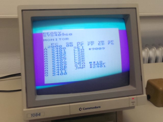
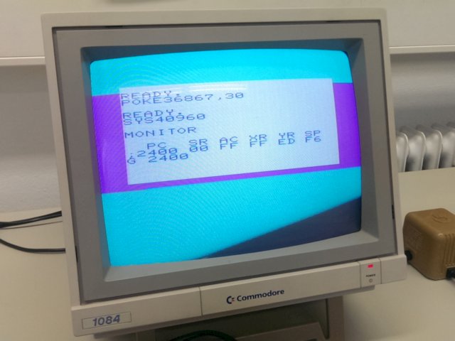
You see the used program in the top photo. I set the paddle to a position that resulted in a readout value for a purple border in the video DMA range, and cyan colour everywhere else: the top 3 bits of the POTY register are shifted into the bottom 3 bits of the border/background register. You also see the update rate *and* vertical position is strongly linked to text screen lines, i.e. every 8 rasters - and their vertical position is stable.
The POT registers are latched somewhere in the last raster of a text line, so their value is still that of the top border during most of the first text line, but then the value changes. Likewise you see a delay at the bottom border, where the 'border value' only appears when it is latched at the end of the first 'non-DMA' text line. The bottom photo shows a cross-check regarding the influence of the video DMA. As I shorten the display height, so is the purple portion of border colour shortened.
Greetings,
Michael
P.S. my test program above samples the POT register every 23 (=4+5x2+2+4+3) cycles, which is fast enough to catch any vertical drifts of POT register updates (there aren't any). I did a SEI but otherwise did not bother to suppress NMIs - under these circumstances the RESTORE key is the only NMI source.
a few remarks on your latest investigations:
Those *are* the two "tiny" ones on the mainboard - 1 nF as per schematics - which are charged over the pot and measured/discharged by the VIC chip. It would be wasteful to integrate them onto the chip die, and the chip die photos also do not indicate any of such a presence (converse to what you see with the 30 pF 'fudge' capacitor of the 741 OpAmp, for example).JonBrawn wrote:I think that it is charging "a capacitor" (not the tiny one on the board) [...]
What I actually first attributed to an influence by the VSync was not any short charging cycle, but rather the period of the glitches as readable from the POT% registers and as displayed by Paddlescope.As you can see, a short charge cycle. Mike's writeup had mentioned that it was at around the frame refresh frequency, [...]
In the meantime I also found that the paddle readout period is not 512 µs as I had conjectured when writing Paddlescope. Rather the value changes every 8 raster lines, which is 568 cycles on PAL and should be 520 cycles on NTSC. Thus, Paddlescope still is guaranteed to display every distinct value that appears in the registers, but might fetch some of them twice.
Now, 312 raster lines per frame on PAL is divisible by 8 (312/8 = 39), but 261 on NTSC (non-interlaced) isn't. This is likely the reason, the NTSC VIC has that irregularity in the charge cycles: it resyncs them to the frame timing on every VSync.
Further investigations by me strongly link the glitches to the parts of the screen where video DMA happens - i.e. the active part of the display window, but not the top/bottom border:
You see the used program in the top photo. I set the paddle to a position that resulted in a readout value for a purple border in the video DMA range, and cyan colour everywhere else: the top 3 bits of the POTY register are shifted into the bottom 3 bits of the border/background register. You also see the update rate *and* vertical position is strongly linked to text screen lines, i.e. every 8 rasters - and their vertical position is stable.
The POT registers are latched somewhere in the last raster of a text line, so their value is still that of the top border during most of the first text line, but then the value changes. Likewise you see a delay at the bottom border, where the 'border value' only appears when it is latched at the end of the first 'non-DMA' text line. The bottom photo shows a cross-check regarding the influence of the video DMA. As I shorten the display height, so is the purple portion of border colour shortened.
Lance should be reachable over Denial's PM system, but he hasn't been active for quite some time now.At this point I'd need to call on someone like Lance Ewing to discuss what is going on in the area around the counters and latches that implement this circuit inside the 6560. Does anybody know how I can contact him?
Greetings,
Michael
P.S. my test program above samples the POT register every 23 (=4+5x2+2+4+3) cycles, which is fast enough to catch any vertical drifts of POT register updates (there aren't any). I did a SEI but otherwise did not bother to suppress NMIs - under these circumstances the RESTORE key is the only NMI source.