
lance.ewing wrote:were you able to prove that when you read the POT values outside of the text window, that the jitter was not present?
Here we go:Mike wrote:For the big spikes, their duty time is more or less exactly the same time no DMA is done. If they were coupled to the VBLANK period, they'd only be half as wide. If I find time next week, I can re-check on real h/w that these spikes exactly correspond to the non-DMA time.
A sample output of Paddlescope on POTY: You can clearly see the downward spikes/glitches, which are roughly one character wide. The gap in the middle of the screen comes from the update cycle. Some other noise that's also present has a peak-peak value of around 4..6 pixels, but those spikes "jump" by roughly 16 pixels, or even more!
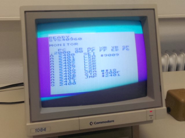
To see the coupling of those spikes with the screen DMA, I typed in a small program into the monitor:
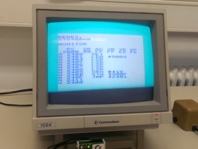
The program shifts the paddle value by 5 bits to the right, ORs in #$18 (white background, non-inverted) and writes the result into the border/background colour register. It's quite easy to find paddle positions, where the border colour differs between DMA and non-DMA parts of the screen:
As you found out, the paddle value is indeed latched on each 8th raster. The first text line has the "non-DMA value" because its "measurement" took place while the DMA was off. Same applies to the 8 rasters below the text window, where the "DMA value" is readable in POT% for 8 rasters after screen DMA end.
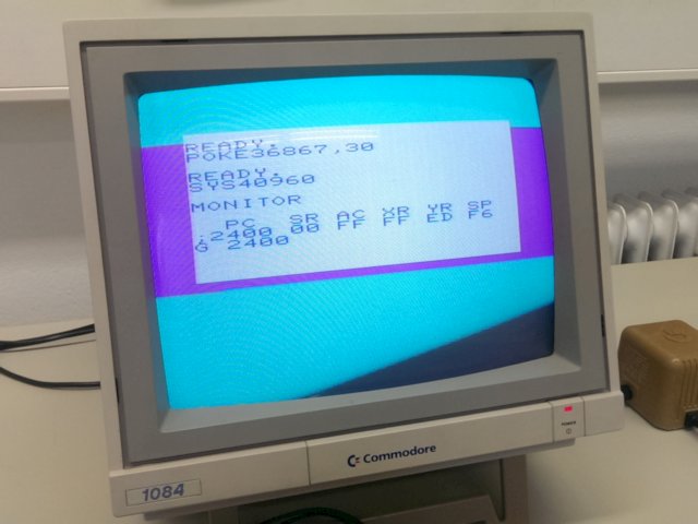
Finally, cross-check with a shortened text screen:
My proposition holds - with two results:
1. There are extra glitches most promiment on POTY, that are definitely coupled to the non-DMA ./. DMA time of screen display.
2. (not shown:) The "minor" noise on POTX has roughly *twice* the peak-peak value compared to POTY, but doesn't show those glitches as prominently. That corresponds well with the geometry/length of the BIAS interconnect!
Greetings,
Michael
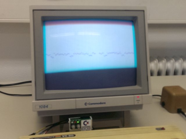
P.S. sorry for the fuzzy photos. This time I only had my mobile phone handy.