Full size here: http://oms.wmhost.com/misc/sid_filter.gif
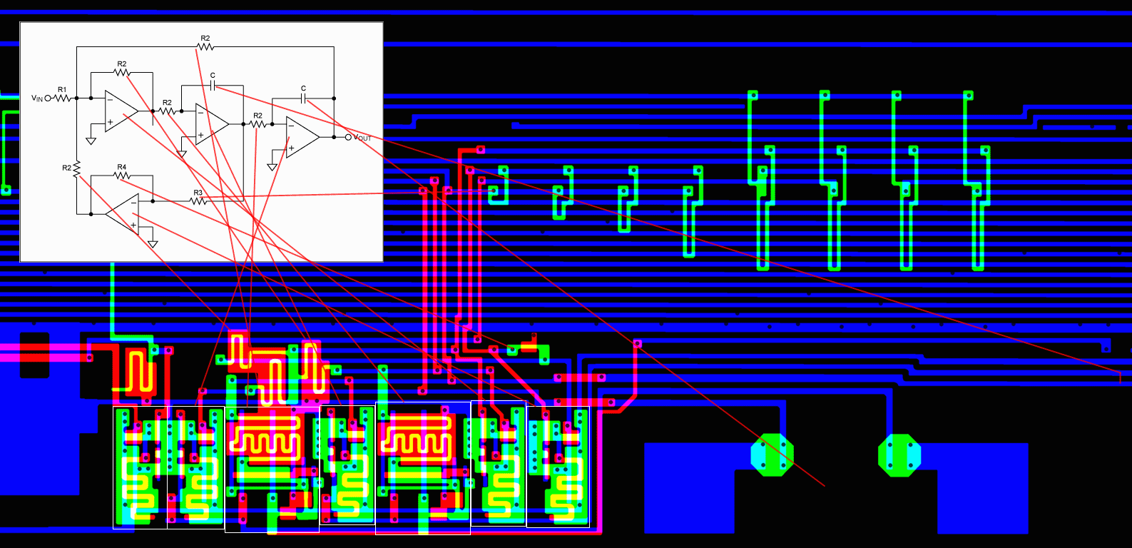
And should you find something like this well it appears to be a FET OP-AMP:
There must be a number of these in the 6560/61 design as well.
Moderator: Moderators

To make things a bit clearer, I've created a version of the image in the previous post that is illustrating the concept of the resistance being by square area. I've done this by laying out little white squares along the lengths of each of the resistors.lance.ewing wrote:They go on to say that this equates to 10000 ohms per square area. Apparently it doesn't matter what the size of the square is.
Makes perfect sense to me: if a surface area of a conductive material is larger, you have more pathway to conduct so you have to compensate by making it longer to re-increase resistance.lance.ewing wrote:They go on to say that this equates to 10000 ohms per square area. Apparently it doesn't matter what the size of the square is.
And you can see the 2nd tiled pathway to the right has been intentionally stretched a bit longer.To make things a bit clearer, I've created a version of the image in the previous post that is illustrating the concept of the resistance being by square area. I've done this by laying out little white squares along the lengths of each of the resistors.
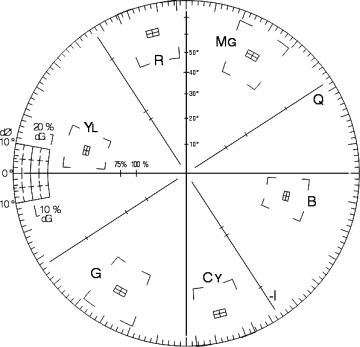
I think you're right on!If we were to label them from left to right as 1, 2, 3 and 4, then I believe that these are the angles for those:
1 = 180 (Yellow)
2 = 0 (Blue)
3 = 270 (approx a Cyan colour, but not exactly the VIC cyan)
4 = 90 (approx a Red colour, but not exactly the VIC red)
I'm only just learning this as I'm going along, but I assume that the Blue would be the SIN one? The Yellow the /SIN? The Red the COS? The Cyan the /COS? Correct me if you think that's wrong.
This implies you never need to sum more than 2 of them to get the color you want.The amplitudes of the two waveforms are apparently controlled by this and work together to determine the phase shift. To quote what Bob Yannes said:
"An analog summer was used to create the phase-shifts in the Chroma signal by adding together the appropriate two waveforms at the appropriate amplitudes. The Color Palette data went to a look-up table that specified the amplitude of the waves by selecting different resistors in the gain path of the summer. The end result was that we could create any hue we wanted by looking at the NTSC color wheel to determine the phase-shift and then picking the appropriate resistor values to produce that phase-shift."
This seems very much like what we're seeing in the 6561 die shot, except that it's obviously PAL we're looking at.
I don't think you have to go that far. I think it's worth it to compare the lengths of resistors relative to one another and that will give you how much of SIN and how much of COS, etc... is in a color. However, given what I said above, the length to width ratio appears completely irrelevant. I really think what matters is the length of one vs the length of the other.Placing those white boxes was a temporary thing to get a rough idea. What I want to do now is measure the relative resistance more accurately, by working out as close as I can get how many times longer each resistor is than its width. The ratio between the numbers determined for the two resistors used for each colour should in theory allow the phase shift to be worked out. Might take a bit of math though.
Excessively pure colors don't display well in both NTSC and PAL. When creating colors in Photoshop using the HSV system, colors with high luminance can easily trigger an excessive saturation warning (the little '!' symbol ) which indicates the color chosen cannot be displayed accurately.A few interesting things to note: Although the VIC-I Yellow and Blue colours are in theory at 180 and 0, the die shot shows that they still select two of the waveforms, and that they are still mixing those together. But the difference in the resistor lengths is quite large, so that although Yellow is selecting both the 180 and 90 waveform lines, it is very strongly weighted towards the Yellow (the resistor used with the 90 line is 25 squares long, whereas the resistor used with the 180 line is just over 4 squares long). I guess what this might mean is that in theory Yellow is ever so slightly off the 180 line. Something similar must be true of Blue.
Same as above.In the case of Orange, the number of squares of length of the two resistors is roughly the same, which is what we'd expect, since it is halfway between the two angles. Strangely though, Purple and Green do not appear to be weighted evenly between their two waveforms.

not quite - if you violate those specs you either dont get an image (because bursts are not detected) or nothing happens at all (out of gamut colors simply dont show).It's very likely the FCC in the US and whatever communication comission in Europe would have prohibited the sales of the VIC-20 and C64 if these machines were to send signals to television sets beyond their acceptable limits.
PLA dissected is a nice document but it is about a strictly digital IC.lance.ewing wrote:Pages 47-49 of the C64 PLA Dissected document appear to be relevant here in determining how the capacitor works. It shows three different capacitors, all three of which have a similar overlap pattern that I'm seeing in the images we've been looking at above, so I'm confident now that it is a capacitor that we're seeing. Hopefully I can use the C64 PLA Dissected doc to help work out the schematic.
I think those pages have pointed me in the right direction though. On page 47, it talks about RC low-pass filters, and through reading up on those, I've realised that the integrators I've been looking at in the images above may not have op-amps in them at all. They could be simple RC integrators like those described on the following pages:eslapion wrote:PLA dissected is a nice document but it is about a strictly digital IC.