FPGA replacement for VIC I chip?
Moderator: Moderators
-
lance.ewing
- Vic 20 Afficionado
- Posts: 413
- Joined: Sat Nov 10, 2012 3:19 pm
- Website: https://sites.google.com/site/mos6561vic/
Re: FPGA replacement for VIC I chip?
I did a bit of searching online after my most recent post, for search phrases such as "inverter with resistive feedback", or "inverter as an amplifier". There are a lot of interesting search results in there. I see things like "self-biasing", and "operating within the linear region" being mentioned. A couple of sites talk about turning an inverter in to an amplifier by connecting a resistor from the output to the input. Most of the talk is in relation to CMOS inverters, but perhaps it also applies to NMOS.
-
lance.ewing
- Vic 20 Afficionado
- Posts: 413
- Joined: Sat Nov 10, 2012 3:19 pm
- Website: https://sites.google.com/site/mos6561vic/
Re: FPGA replacement for VIC I chip?
I'd like to return momentarily to my post on Monday evening. In it I mentioned the BLANKING line that would be 1 if either horizontal or vertical blanking is currently in progress. It was also mentioned that when BLANKING is 1, and COL BRST is 1, the colour output is enabled. The Colour Burst only applies during horizontal blanking though.
I've found an interesting logic block related to this. It is as follows:
There are a couple of things going on here: The first is the calculation of the BLANKING value.
That is relatively straight forward. You'll notice though that there are two poly lines coming off the V.BLANK metal to poly contact. The poly line that goes upwards appears to be what pulls the COL BRST line low when vertical blanking is in progress. This might suggest that whatever it is that generates the colour burst 1 value on that COL BRST line, it perhaps continues to do it during vertical blanking, and therefore it relies on this transistor to pull it down to 0. That's my assumption. I can't see why it would be needed otherwise.
I've found an interesting logic block related to this. It is as follows:
- beyond_shift_reg_30_logisim_1.png (6.86 KiB) Viewed 1496 times
-
lance.ewing
- Vic 20 Afficionado
- Posts: 413
- Joined: Sat Nov 10, 2012 3:19 pm
- Website: https://sites.google.com/site/mos6561vic/
Re: FPGA replacement for VIC I chip?
Returning now to the composite colour output, this is the lower part of that zoomed out image I posted two days ago:
I'm going to talk this one through in a bit more detail. The three pink arrows show where the input for this block is coming from. The first pink arrow towards the top middle shows where the output is coming in from the part of the die shot that we were discussing on Tuesday. It follows that metal line down to the metal to diffusion contact on the right mid. After switching to diffusion, the diffusion line passes through a resistor. It then gets to a buried contact (the blue box) and switches to a polysilicon line at that point. Note that the diffusion line coming in to that same buried contact from the right appears to be a resistive feedback path, as far as I can tell.
The polysilicon line connects to the gate of a largish transistor. The polysilicon passes over the diffusion area of this transistor and weaves it way down to the bottom again. Notice to the left of this transistor gate (i.e. to the left of the polysilicon) there is another buried contact connecting to the gate of a smaller transistor. This appears to be the normal gate to source connection for a depletion mode pull up transistor. The tell tale signs are both the gate to source connection, and the VDD contact above that transistor. The combination of the larger enhancement mode transistor and depletion mode transistor form an inverter. Its from the end of that short polysilicon line across the gate of this depletion mode transistor that there is a resistive feedback path back to the input of this inverter. The reason this is the output of that inverter is due to the gate to source buried contact.
To the left, the output of that inverter connects to the gate of another transistor. I can't visually tell if this transistor is a depletion mode transistor or not. VDD is connected to its drain, so it appears to be a pull up, but due to the gate's very wide short shape, it doesn't look any different visually from the wide short enhancement mode transistors in this same image. It is quite possible that this pull up is an enhancement mode transistor, but I can't be sure at the moment either way.
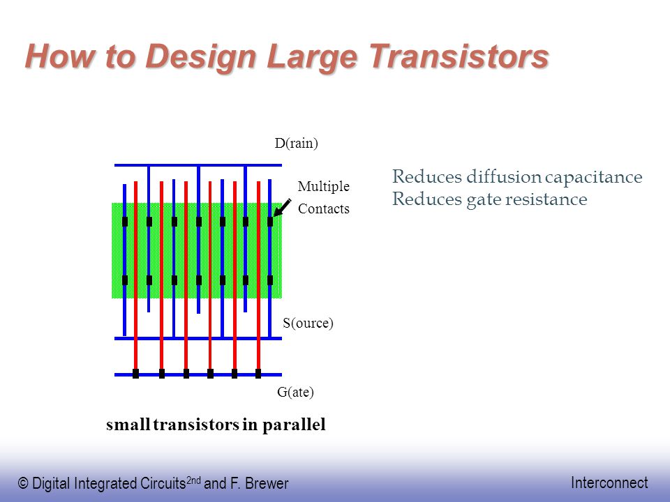
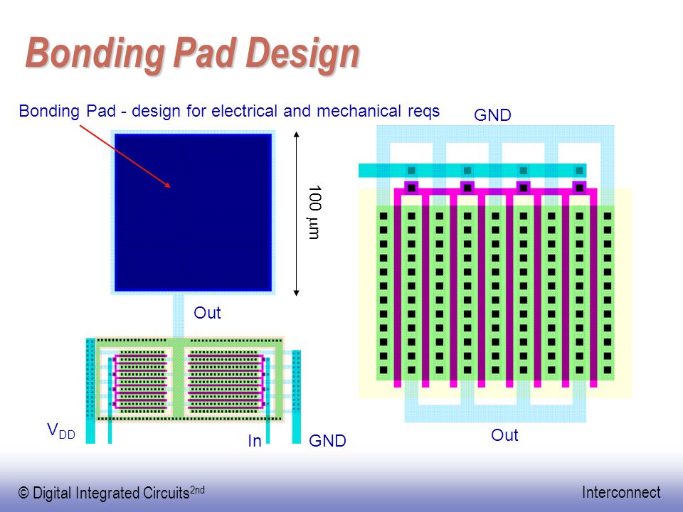
We now get to a strange looking finger shaped structure. It looks like lots of enhancement mode transistors in parallel, and actually that's what it technically is, but the whole thing can be viewed as a single very large transistor. If you read what is online about bonding pad output driver design, you'll see it mentioned a few times that this is the strategy they use.
http://images.slideplayer.com/17/535733 ... ide_83.jpg
http://images.slideplayer.com/16/493286 ... ide_20.jpg
So all those finger like red polysilicon lines passing over the large diffusion area are essentially the gate of this very large transistor. The input to that gate is connected to the input of the first inverter that we discussed above. All those metal "fingers" with VSS contacts on them are the source of the very large transistor, and the two metal "fingers" with the unlabelled metal to diffusion contacts on them are the drain of the very large transistor. In combination with the smaller transistor we mentioned before discussing this large transistor, it appears to form a large inverter. The drain of the large transistor is the output of that inverter and it leads directly to the bonding pad labelled Chrom.
The schematic for this rather complex layout is actually quite simple. When I get a chance later on today, I'll try to draw the schematic and include it here.
The polysilicon line connects to the gate of a largish transistor. The polysilicon passes over the diffusion area of this transistor and weaves it way down to the bottom again. Notice to the left of this transistor gate (i.e. to the left of the polysilicon) there is another buried contact connecting to the gate of a smaller transistor. This appears to be the normal gate to source connection for a depletion mode pull up transistor. The tell tale signs are both the gate to source connection, and the VDD contact above that transistor. The combination of the larger enhancement mode transistor and depletion mode transistor form an inverter. Its from the end of that short polysilicon line across the gate of this depletion mode transistor that there is a resistive feedback path back to the input of this inverter. The reason this is the output of that inverter is due to the gate to source buried contact.
To the left, the output of that inverter connects to the gate of another transistor. I can't visually tell if this transistor is a depletion mode transistor or not. VDD is connected to its drain, so it appears to be a pull up, but due to the gate's very wide short shape, it doesn't look any different visually from the wide short enhancement mode transistors in this same image. It is quite possible that this pull up is an enhancement mode transistor, but I can't be sure at the moment either way.
We now get to a strange looking finger shaped structure. It looks like lots of enhancement mode transistors in parallel, and actually that's what it technically is, but the whole thing can be viewed as a single very large transistor. If you read what is online about bonding pad output driver design, you'll see it mentioned a few times that this is the strategy they use.
http://images.slideplayer.com/17/535733 ... ide_83.jpg
http://images.slideplayer.com/16/493286 ... ide_20.jpg
So all those finger like red polysilicon lines passing over the large diffusion area are essentially the gate of this very large transistor. The input to that gate is connected to the input of the first inverter that we discussed above. All those metal "fingers" with VSS contacts on them are the source of the very large transistor, and the two metal "fingers" with the unlabelled metal to diffusion contacts on them are the drain of the very large transistor. In combination with the smaller transistor we mentioned before discussing this large transistor, it appears to form a large inverter. The drain of the large transistor is the output of that inverter and it leads directly to the bonding pad labelled Chrom.
The schematic for this rather complex layout is actually quite simple. When I get a chance later on today, I'll try to draw the schematic and include it here.
-
eslapion

- ultimate expander
- Posts: 5458
- Joined: Fri Jun 23, 2006 7:50 pm
- Location: Canada
- Occupation: 8bit addict
Re: FPGA replacement for VIC I chip?
AFAIK, what you call V. Blank and H. Blank should be called V. Sync and H. Sync
Of course, a color burst signal is only needed during H. Sync and only during a specific portion of it.
Of course, a color burst signal is only needed during H. Sync and only during a specific portion of it.
Be normal.
-
lance.ewing
- Vic 20 Afficionado
- Posts: 413
- Joined: Sat Nov 10, 2012 3:19 pm
- Website: https://sites.google.com/site/mos6561vic/
Re: FPGA replacement for VIC I chip?
The H.BLANK and V.BLANK labels that I've used are short for Horizontal Blanking and Vertical Blanking, as described here:
https://en.wikipedia.org/wiki/Horizonta ... g_interval
https://en.wikipedia.org/wiki/Vertical_ ... g_interval
The H.Sync and V.Sync are short pulses that happen within the relevant blanking interval:
http://www.kramerelectronics.co.uk/acad ... SyncPulses
There is quite a good Glossary at the bottom of the following web page that defines both blanking and sync pulses:
https://www.maximintegrated.com/en/app- ... mvp/id/734
If you look at page 16 in the 6560/6561 datasheet, you'll see a diagram that shows both the blanking interval and the horizontal sync.
Edit: I think this entry from the Glossary mentioned about is the most relevant:
Blanking Interval: There are horizontal and vertical blanking intervals. Horizontal blanking interval is the time period allocated for retrace of the signal from the right edge of the display back to the left edge to start another scan line. Vertical blanking interval is the time period allocated for retrace of the signal from the bottom back to the top to start another field or frame. Synchronizing signals occupy a portion of the blanking interval."
-
lance.ewing
- Vic 20 Afficionado
- Posts: 413
- Joined: Sat Nov 10, 2012 3:19 pm
- Website: https://sites.google.com/site/mos6561vic/
Re: FPGA replacement for VIC I chip?
The following is what I think the schematic is for the most recent section of the die shot that we were looking at earlier today:
The red dot on the right hand side is the input and the red dot on the left hand side is the output (i.e. the metal line that connects to the bonding pad). Q3 is the very large transistor that is formed out of a number of smaller transistors in parallel.
As noted previously, I can't tell whether the Q4 transistor is a depletion mode or enhancement mode transistor. It looks like an enhancement mode transistor, so I've drawn it like that. The four transistors are connected like an inverting super buffer, but Q4 would usually be a depletion mode transistor for an inverting super buffer, so I'm not certain what you'd call this one.
I simulated the above circuit in Proteus and what it seems to do is invert and amplify, which I think is what we were expecting. You'll recall that the section of the die shot leading up to this section had an inverter that also had resistive feedback, and actually I see now that it also has the equivalent of R2. It seems to me that when SHADE is 0, that previous inverter would be reducing the amplitude, whereas if SHADE is 1, it would be increasing the amplitude, which is once again what we'd be expecting (I think). It would also have inverted the wave form, and so the above circuit would be reversing that inversion.
- beyond_shift_reg_28_schem.png (6.65 KiB) Viewed 1450 times
As noted previously, I can't tell whether the Q4 transistor is a depletion mode or enhancement mode transistor. It looks like an enhancement mode transistor, so I've drawn it like that. The four transistors are connected like an inverting super buffer, but Q4 would usually be a depletion mode transistor for an inverting super buffer, so I'm not certain what you'd call this one.
I simulated the above circuit in Proteus and what it seems to do is invert and amplify, which I think is what we were expecting. You'll recall that the section of the die shot leading up to this section had an inverter that also had resistive feedback, and actually I see now that it also has the equivalent of R2. It seems to me that when SHADE is 0, that previous inverter would be reducing the amplitude, whereas if SHADE is 1, it would be increasing the amplitude, which is once again what we'd be expecting (I think). It would also have inverted the wave form, and so the above circuit would be reversing that inversion.
-
lance.ewing
- Vic 20 Afficionado
- Posts: 413
- Joined: Sat Nov 10, 2012 3:19 pm
- Website: https://sites.google.com/site/mos6561vic/
Re: FPGA replacement for VIC I chip?
I think we're ready to start looking at the circuitry leading up to Pin 3 (i.e. what the datasheet calls the Composite Sync and Luminance pin). The journey in this direction begins with the SHADE line. You'll remember that it was used as part of generating the output for Pin 2 (being the Chrom. output). Well that particular metal line continues on towards the Sync/Luminance part of the die shot.
In the middle at the top, you can see a metal to poly contact with a label of SHADE. The is the input to this block. Slightly to the right of this, you can see two metal to diffusion contacts, also both labelled SHADE. That is the output of this block. Doesn't take much to assume from those input and output labels that this block logically does nothing, i.e. the input is the same as the output. It would certainly have a very important purpose though, but for now let's look at the logic diagram for this block:
I've used the symbol that Skoe used in his C64 PLA document for the inverting super buffer. Logically it is four inverters in a row. The first three are simple inverters. The fourth one is an inverting super buffer. If you invert a logic level four times, the output ends up being the same as the input.
So why does it need to do this? Unfortunately I don't know enough about NMOS design and fabrication to answer this, but I have read a bit about things like level restoration, propagation delay, gate capacitance, timing, fan out, and things like this. In addition to the functional logic, inverters are also used in a number of ways to solve various electrical issues within the IC that logically may appear to do nothing, but that the circuit will fail to work without. These are things I'm not really focussing on, as it seems quite a complex topic. Instead I'm trying in the most part to focus on the logical functionality.
I'm guessing that at some point I'm going to need to understand a bit about propagation delay though. I've read that IC designs can rely on the propagation delay of certain parts of a circuit for timing purposes. Timing is something that is important to the logical functionality.
-
lance.ewing
- Vic 20 Afficionado
- Posts: 413
- Joined: Sat Nov 10, 2012 3:19 pm
- Website: https://sites.google.com/site/mos6561vic/
Re: FPGA replacement for VIC I chip?
I'm going to move on quite quickly to the next post, because they're related. If we look to the right of the section of the die shot that we were looking at in the last post, we see the following:
It all looks very interesting at first. We see the seven colour control lines coming down from the top. If you recall, each of the colour control lines split in to three. Two of those headed upwards toward the sine/cosine generators and resistors to control generation of the composite colour output. The other set of seven lines headed downwards towards the luminance part of the die shot. This is now what we're looking at.
So what we have are seven structures with the exact same layout, one for each of the colours, starting at the left hand side for Cyan, Purple, Red, Green, Orange, Blue, and Yellow.
The reason this post is related to the previous post is because the logic diagram for each of those seven blocks is that same as what we saw for the SHADE signal, i.e. they each have three inverters followed by an inverting super buffer. I'm not going to repeat that image here since you can simply look up at the previous post to see it.
This stresses the importance of what we discussed towards the end of the previous post. Inverters are used for very important reasons other than functional logic. We can see here that quite a large area has been devoted to this, in fact the more I see of this die shot, the more I realise that a considerable amount of the die shot is taken up by such inverters.
These three inverters followed by the inverting super buffer for each colour line are primarily here to drive the luminance part of the die shot.
I have labelled the output contact for each of the seven colours and you can see that they all head off along metal lines towards the right and off the image. It is also worth noting that we can see the continuation of the SHADE metal line towards the top, also heading towards the right. This is from the output of what we saw in the previous post.
There are five other metal lines heading towards the right. Two of these are VSS, one of them is VDD. Those are all labelled. There are two that are not labelled in this particular image, i.e. the two between the VDD and VSS lines towards the top. The metal line immediately above VDD in this image is the BLANKING line. The metal line above that I am currently thinking might be the SYNC line. It may take a while before I can prove that one way or the other though.
The area to the right of this image is certainly going to be interesting.
-
eslapion
- ultimate expander
- Posts: 5458
- Joined: Fri Jun 23, 2006 7:50 pm
- Location: Canada
- Occupation: 8bit addict
Re: FPGA replacement for VIC I chip?
There are other custom Commodore chips which are saturated with double and triple inverters in sequence. Usually it is to make sure something happens slightly after or before a specific clock signal.lance.ewing wrote:I've used the symbol that Skoe used in his C64 PLA document for the inverting super buffer. Logically it is four inverters in a row. The first three are simple inverters. The fourth one is an inverting super buffer.
In this specific case, I would guess it is to ensure the luma/sync signal is perfectly in tune with the chroma signal.
Be normal.
-
lance.ewing
- Vic 20 Afficionado
- Posts: 413
- Joined: Sat Nov 10, 2012 3:19 pm
- Website: https://sites.google.com/site/mos6561vic/
Re: FPGA replacement for VIC I chip?
Yeah, I'd imagine it will be something like that. I'm not going to spend time trying to work that out at this point though. What I envisage is that I'll work my way through the whole chip in the fashion I've been doing over the past few months, and by then I will have absorbed a lot more knowledge on how things are working in these chips, and hopefully I will have passed this on to many of you through these posts. It seems that with each new section, I've been discovering something new regarding die shot analysis. Each quarter will probably take three months at this rate, so the whole thing taking roughly a year. And then comes the second pass I guess, i.e. the pass that determines things like transistor sizes, delays, timing, and that kind of thing.
We can view the 6561 die chip in roughly four quarters. The quarter I've been looking at to date is in the bottom right corner. This quarter is focussed mainly on the video generation. We're getting quite close now to completing this quarter, but I'd imagine it will probably take a month or so more to complete, and then I'll move on to one of the other quarters. In the top left quarter is the address computation for fetching data. In the bottom left hand quarter are the vertical and horizontal counters, and the logic that generates things like the blanking, sync, and colour burst signals, and towards the bottom of that quarter is where some of the clocks originate. In the top right quarter are the tone generators and Pot X and Pot Y registers. Most of the other control registers are along a horizontal section in the lower part of the top half of the die shot, so form part of the top two quarters.
I think I'm ready to talk through the luminance part of the die shot now, so hopefully there will be another post later this evening on the first parts of this.
-
lance.ewing
- Vic 20 Afficionado
- Posts: 413
- Joined: Sat Nov 10, 2012 3:19 pm
- Website: https://sites.google.com/site/mos6561vic/
Re: FPGA replacement for VIC I chip?
The following image is the first part of the luminance section of the die shot:
Open that image in full size in another tab. We'll start discussing this by looking towards the top left. There is a metal to poly contact there that I have put the label "SYNC ??" on. The only reason I've added the ?? to the label is because I haven't yet worked out the logic that generates the pulses on that line to be certain it is the SYNC line. But through a process of elimination, I'm fairly certain it must be the SYNC line. So let's proceed with the assumption that this contact does have the SYNC signal on it. I'm assuming that this signal will be active (or high) whenever there is a sync pulse of any kind (whether it be the vertical sync pulse, equalising pulses, or horizontal sync pulse).
That metal to poly contact labelled SYNC is connected to the gate of a transistor. This transistor gate is very wide and it weaves around in a serpentine manner. If this serpentine pattern had been in an area that wasn't over diffusion, then it would have been identified as a resistor. But given that this is over diffusion then it is clearly the gate of a transistor. My gut tells me that the serpentine pattern of the gate is important but at the current point in time I'm not sure what that importance is. The serpentine layout basically means that the transistor gate is VERY wide (but also very short in length). This is one of those things that will need revisiting on a second pass of the die shot.
We're going to have to make more assumptions at this point. If we look over the 6560/6561 datasheet, we'll see that the lowest level that is output on the luminance/sync pin is when there is a sync pulse. What we can assume then is that when SYNC is active, this transistor causes the output to drop to the lowest level. Those four metal to diffusion contacts that are surrounded by the serpentine shaped transistor gate are at the start of a metal line that leads directly to the luminance/sync bonding pad. The assumption therefore is that when SYNC is high, it pulls the luminance/sync output to it's lowest level.
This covers the left hand side of the above image.
The right hand side is related to BLANKING and BLACK. A quick check of the 6560/6561 datasheet shows that the luminance/sync output pin is at the same level for both the BLANKING periods and when the colour is BLACK. This level is higher than the SYNC level though.
There is a bit of logic in this particular case. There is a NOR gate (top middle of the image) that has the BLANKING and BLACK signals as inputs. The output of that NOR gate passes through an inverter. The net effect is an OR. So towards the bottom of the right hand side of the image, we see a pink arrow and a label that says "BLANKING OR BLACK". This BLANKING/BLACK output is connected to the input of another serpentine shaped transistor gate. The drain of this transistor is connected to a poly line with a pink arrow showing the direction towards a metal to poly contact. Once again my gut tells me that the shape of the gate is important, but as yet I don't know what the significance is. What we can see though is that this transistor gate is not as wide as the SYNC transistor gate. It is possibly to do with how low the level drops. I can't see anything else other than the difference in width of the transistor gates that can explain why the SYNC signal makes the output drop lower than the BLANKING/BLACK signal.
-
lance.ewing
- Vic 20 Afficionado
- Posts: 413
- Joined: Sat Nov 10, 2012 3:19 pm
- Website: https://sites.google.com/site/mos6561vic/
Re: FPGA replacement for VIC I chip?
Let's move right along. This time I'm going to take a larger chunk of the die shot than I'd normally cover, mainly because the three sections of this image are very similar:
We can view this image in three sections. On the left hand side is the luminance generation for the CYAN colour. In the middle is the luminance generation for the PURPLE colour, and on the right is the luminance generation for the RED colour. In each case there is a metal to poly contact with a label on it that has the colour name. In each case there is also another metal to poly contact with the label SHADE. You will remember that for each colour, there are two shades: the darker version of the colour and the lighter version of the colour. The SHADE contact in each case is controlling the selection between the dark and light shade of the colour. A value of 0 is the lighter shade and 1 is the darker (note that this is the opposite of what you might initially assume).
The colour labelled contact, and the SHADE labelled contact, are both connected to the gate of transistors. Let's take CYAN as an example. If SHADE is off, but CYAN is on, then it is the luminance for the lighter shade of CYAN that is being output (since SHADE is on for the darker shade and off for the lighter shade). In this scenario, the drain of the transistor whose gate has the CYAN signal on it is connected to a long serpentine shaped resistor. This type of resistor is a polysilicon only resistor. In previous posts we've seen transistor gates being used as resistors, and in those cases the resistance per square has been something like 10K ohm. The resistance of a polysilicon line is between 15 to 100 ohms per square area, so quite a bit smaller. The serpentine shape of the resistor means that the polysilicon line is very long and also very narrow. So the ratio of length to width is quite high, and therefore the number of "squares" is quite high.
In each of the three cases (i.e. CYAN, PURPLE and RED luminance generation), there is a buried contact shown part way along the long serpentine resistor, so it is actually two resistors. If SHADE is off then the two resistors can be viewed as one very long serpentine resistor, the number of "squares" of which contributes directly to the resistance. The higher the resistance value, the higher the voltage output on the luminance/sync pin (due to it being open drain). So when SHADE is off, the resistance is higher, which means the voltage is higher and the luminance is therefore higher.
When SHADE is on, then the output of the SHADE transistor is connected to that buried contact. This in effect turns the long resistor in to the two shorter resistors, one of which is now in parallel with the SHADE transistor, which effectively negates the resistance of that resistor. The resistance rather than being the two resistor values added in series is now almost all made up of the second resistor. It is this shortening of the resistance that causes the luminance level to go lower for the darker shade of the colour.
This post is an introduction to the colour luminance section of the die shot. I hope that in the next post I will have measured the lengths of the serpentine resistors for each colour and can see how this relates to the different levels of luminance.
Edit: I corrected a couple of points above. I had said initially that when SHADE is off, it is the darker shade of the colour, but looking back at the logic that generates that value, it is actually off for the lighter shade and on for the darker shade. This makes a lot more sense with regards to this luminance section. The longer resistance (when SHADE is off) actually creates the higher output voltage.
Last edited by lance.ewing on Sat Jun 18, 2016 4:28 pm, edited 2 times in total.
-
lance.ewing
- Vic 20 Afficionado
- Posts: 413
- Joined: Sat Nov 10, 2012 3:19 pm
- Website: https://sites.google.com/site/mos6561vic/
Re: FPGA replacement for VIC I chip?
Here is what Bob Yannes said about luminance in the VIC-II:
I haven't yet had a chance to work out the length of the resistors in "squares". It might be easiest to overlay a grid to aid in that counting.
Once again this seems to apply to the VIC-I as well. The luminance/sync output is open drain in the 6561, and what we were seeing in the most recent image are transistors for each colour being used to switch in different pull down resistors.Luminance was controlled using a simple voltage divider which switched different pull-down resistors into the open-drain output. We could create any Luminance we wanted by choosing the desired resistor value.
I haven't yet had a chance to work out the length of the resistors in "squares". It might be easiest to overlay a grid to aid in that counting.
-
lance.ewing
- Vic 20 Afficionado
- Posts: 413
- Joined: Sat Nov 10, 2012 3:19 pm
- Website: https://sites.google.com/site/mos6561vic/
Re: FPGA replacement for VIC I chip?
The grid approach is somewhat error prone, in that I can't be certain I haven't missed counting a square, or counted a square twice. There are hundreds of squares to count in each case. So I'm now going with the approach of asking Inkscape how long the path is. I'm drawing a path along the middle of the serpentine resistor and asking Inkscape how long that is. I can then work out how many squares that equates to.
-
lance.ewing
- Vic 20 Afficionado
- Posts: 413
- Joined: Sat Nov 10, 2012 3:19 pm
- Website: https://sites.google.com/site/mos6561vic/
Re: FPGA replacement for VIC I chip?
I've finished measuring the lengths of the pull down resistors for each colour now, both the shorter and the longer in each case.
In the process of doing this, I've realised that the resistance of the two transistors that are involved may play more of a part in the overall resistance of the pull down than what I had previously been thinking. As we've previously noted in this topic, the resistance per square of a switched on transistor gate is somewhat larger than a polysilicon line, e.g. 10K ohms versus something like 15-100 ohms. The length to width ratio of these transistors is quite small, but even so, my rough estimate after having a closer look at it suggests to me that the SHADE transistor could add up to 10% of the overall resistance that makes up the pull down value, in some instances. It really depends a lot on what the polysilicon line's resistance actually is. The Mead/Conway book says that 15-100 ohms was typical at the time of the publication of the book, which was a few years prior to when the VIC chip was created. The book also states that there are a number of factors than can affect the resistance of the polysilicon and that it depends a lot on the process used as to what the resistance per square is for polysilicon. We really don't know.
The point of the exercise I am currently going through is not to accurately determine what the resistance in ohms might be. It's more to get a rough idea.
But given that this luminance part of the VIC chip is the pull down part of the voltage divider, presumably pin 3 being the mid point of the voltage divider, then the pull up part of the voltage divider is on the VIC 20 board itself. So in theory if you knew the voltages being output on pin 3, and you knew what the resistance of the pull up part of the voltage divider where, then you could work out the resistance of the pull down part for each of the colours. I'm not sure if this is a worthwhile exercise to go through or not. Any thoughts on that?