@lance.ewing
Skoe is just plain brilliant.
If you have difficulty identifying specific components in the 6561, I am sure he is the guy who can help you.
FPGA replacement for VIC I chip?
Moderator: Moderators
-
eslapion

- ultimate expander
- Posts: 5458
- Joined: Fri Jun 23, 2006 7:50 pm
- Location: Canada
- Occupation: 8bit addict
Re: FPGA replacement for VIC I chip?
Be normal.
-
lance.ewing
- Vic 20 Afficionado
- Posts: 413
- Joined: Sat Nov 10, 2012 3:19 pm
- Website: https://sites.google.com/site/mos6561vic/
Re: FPGA replacement for VIC I chip?
Yes, I think it may be time to contact him and hopefully he might be willing to join in the conversation in this thread.
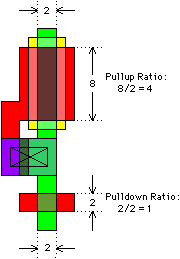
This evening I've been reading up on NMOS transistor gate ratios. The Mead/Conway book states a few interesting things. The first is that the resistive impedance is proportional to the length-to-width ratio Z of a MOS transistor's gate region. In a DC circuit like this, resistive impedance is essentially the resistance. This isn't directly applicable to what I wanted to discuss in this particular post, but it relates to some of the earlier posts. It states that the ratio does determine the resistance, so both width and length of the gate region are important for a MOS transistor that is used as a resistor.
The other interesting bit about length-to-width ratios is with regards to inverters (and NOR and NAND gates and basically any NMOS logic gate I guess). The ratio of the pull up's length-to-width to the pull-down network's length-to-width should be at least 4:1. It mentions this is the Mead/Conway book, but also on this web page here:
http://www.rulabinsky.com/cavd/text/chap05-4.html
which lays things out quite nicely with this diagram:
http://www.rulabinsky.com/cavd/images/fig0514.gif
It may or may not be important to the analysis of what I think are the integrator layouts, but the pull-up length-to-width versus pull-down length-to-width ratio of the inverter is roughly 6.5:1. This initially seemed unusual to me, but then looking at a few of the other inverters where the widths are roughly the same for the pull up and pull down, the ratios are quite often also around the 6:1. So perhaps this is normal (in fact the rule says at least 4:1), and perhaps the very wide enhancement mode transistor in this integrator layout needs to be this wide because it's length is the same as the pull up's length. So due to the ratio calculation, if the length's are the same, it's the width that needs to change to compensate, i.e. making the width of the pull down wider will have the same effect as if the length of the pull up was longer.
-
lance.ewing
- Vic 20 Afficionado
- Posts: 413
- Joined: Sat Nov 10, 2012 3:19 pm
- Website: https://sites.google.com/site/mos6561vic/
Re: FPGA replacement for VIC I chip?
Another thing worth mentioning here is that I noticed on page 40 of the C64 PLA Dissected document that is has a quote from James Redfield:
This is quite a relevant endorsement of the Mead/Conway book, particularly since James Redfield is listed as one of the inventors of the Digital Sine/Consine Generator in that patent.Before joining Commodore, one of the grad courses I had taken was a class in VLSI systems design. That class used a book that was the authority for NMOS circuit design at the time: ‘Introduction to VLSI Systems’ by Carver Mead and Lynn Conway [Mead79]. I would highly recommend that any serious student of early VLSI design methodology purchase a copy of this book if at all possible!
-
eslapion
- ultimate expander
- Posts: 5458
- Joined: Fri Jun 23, 2006 7:50 pm
- Location: Canada
- Occupation: 8bit addict
Re: FPGA replacement for VIC I chip?
... I would highly recommend that any serious student of early VLSI design methodology purchase a copy of this book if at all possible!
For free... http://ai.eecs.umich.edu/people/conway/ ... -V2/V2.pdf
Be normal.
Re: FPGA replacement for VIC I chip?
This has been a very interesting thread so far. Keep up the good work lance!
@eslapion: Thanks for that pdf link! I really wish I had that when we were working on x64sc. Maybe there are some more insights to be found?
@eslapion: Thanks for that pdf link! I really wish I had that when we were working on x64sc. Maybe there are some more insights to be found?
-
lance.ewing
- Vic 20 Afficionado
- Posts: 413
- Joined: Sat Nov 10, 2012 3:19 pm
- Website: https://sites.google.com/site/mos6561vic/
Re: FPGA replacement for VIC I chip?
I've had V3 of that PDF on my phone and kindle for a couple of years now, but I did end up buying a physical copy earlier this year, as I find it a lot easier to flick through and study. Each time I read parts of it, I find that I've learnt a bit more in the interim, probably from studying the 6561 die shot, and reading up on various topics online as part of that, and then I'll come back to the Mead/Conway book and discover that I can now understand something it says that previously went over my head. So it's a good book to keep coming back to for anyone that is trying to work out what is happening in these die shots.
I've found an email address for Skoe on his Easyflash site, so I'll give that a go and see how it goes. Hopefully it's his current one.
I feel like I've taught myself a lot about reversing an NMOS die shot, but to someone like Skoe or Segher, I'd still be very much an amateur. I don't mind doing the donkey work if I can absorb all the knowledge required to do it though. So I'll just keep going and see where I get.
-
eslapion
- ultimate expander
- Posts: 5458
- Joined: Fri Jun 23, 2006 7:50 pm
- Location: Canada
- Occupation: 8bit addict
Re: FPGA replacement for VIC I chip?
This thread is giving me an appetite for creating a completely new video chip for the VIC-20 and/or C64!!!
Be normal.
-
lance.ewing
- Vic 20 Afficionado
- Posts: 413
- Joined: Sat Nov 10, 2012 3:19 pm
- Website: https://sites.google.com/site/mos6561vic/
Re: FPGA replacement for VIC I chip?
I haven't yet had a reply from Skoe, and I also haven't got my head around what the exact circuit is for the integrator. So I'm going to proceed by making a few assumptions along the way.
To recap where we're at, this is a zoomed out view of the area of the die shot where I think the sine and cosine generators live:
At the bottom, we have the four metal lines carrying the four waveforms that we've recently been discussing. As noted previously, these four metal lines all head upwards in parallel. This can be seen in the middle of the image. To the right of those four metal lines (and also passing under them) are ten very similar looking structures. We were looking at the bottom two of these in my post on Friday 20th May. My current belief is that these ten structures are what generates the four waveforms and are used as follows:
Something doesn't quite add up about all of this, and I'm hoping at some point an expert will chip in and make the corrections I think this needs. I'm currently stating that those four items in the list above are the identified waveform generators based solely of the fact that that makes sense given the colour control signals and resistor ratios used when the waveforms are combined. I'm half expecting someone might tell me I've got this completely around the wrong way at some point, but until then we'll proceed on my current assumptions.
To recap where we're at, this is a zoomed out view of the area of the die shot where I think the sine and cosine generators live:
- The bottom two generate the inverse cosine wave.
- The next two above that generate the cosine wave (note that the structures used here are actually identical to what was used for the inverse cosine. The difference between them is that the incoming square waves to each are the inverse of each other).
- The next three above that generate the inverse sine wave.
- The next three above that generate the sine wave (note again that the structures used here are identical to what was used for the inverse sine. The difference is once again that the incoming square waves to each are the inverse of each other).
Something doesn't quite add up about all of this, and I'm hoping at some point an expert will chip in and make the corrections I think this needs. I'm currently stating that those four items in the list above are the identified waveform generators based solely of the fact that that makes sense given the colour control signals and resistor ratios used when the waveforms are combined. I'm half expecting someone might tell me I've got this completely around the wrong way at some point, but until then we'll proceed on my current assumptions.
-
lance.ewing
- Vic 20 Afficionado
- Posts: 413
- Joined: Sat Nov 10, 2012 3:19 pm
- Website: https://sites.google.com/site/mos6561vic/
Re: FPGA replacement for VIC I chip?
So having made a few assumptions in the previous post, I'm going to start looking at the structures to the left of the four metal waveform lines. The first of these I'll look at is the top one, which is shown on the left side of the image below:
The input to this structure is the FC2 signal. As previously noted, this isn't a label that I put there but is instead one that was already on Segher's partially labelled 6561 die shot image. My current assumption is that it is a digital clock signal that is at the same rate as the input clock to the 6561. This is because that is what it needs to be to generate the PAL sub-carrier frequency.
After working out the circuit for this structure, I attempted to simulate it in Proteus. The following is the schematic I used for the top half of the structure:
A few things to note about this before we discuss the logic: In Proteus I chose a particular depletion mode transistor (LND150) and a particular enhancement mode transistor (2N7000). In the schematic, the symbol for each is the same though. This is a little bit unfortunate, but the circuit does behave as it should, since the LND150 is a depletion mode transistor. Let's ignore the fact that Proteus is simulating discrete transistors (since I think the end result is the same).
The input coming in on the left (FC2) is connected to three different transistors. The top part is quite straightforward. Q1, Q2, Q4, and Q5 form an inverting super buffer. The output of this is the red circle at the top labelled FC2' i.e. the inverse of FC2. So logically this has simply inverted the FC2 input (being a super buffer, it is also presumably preparing to drive a higher capacitive load).
The lower part is a bit interesitng. The depletion mode transistor, rather than it's gate being connected to it's source (or to gate of another depletion mode transistor, as is the case in an inverting super buffer), it's gate is instead connected directly to the incoming FC2 signal. I'm not exactly sure why but there is probably a good reason for this. Having simulated it, I can tell you that the lower red circle represents an output that is essentially the same as FC2. So it would seem that the gate could have been connected to it's source. This makes me think that there probably is a good reason that it isn't. For our purposes though, the output at the lower red circle is FC2.
In the next post I'll should the second half of the schematic.
After working out the circuit for this structure, I attempted to simulate it in Proteus. The following is the schematic I used for the top half of the structure:
- beyond_shift_reg_23_proteus.png (10.15 KiB) Viewed 1472 times
The input coming in on the left (FC2) is connected to three different transistors. The top part is quite straightforward. Q1, Q2, Q4, and Q5 form an inverting super buffer. The output of this is the red circle at the top labelled FC2' i.e. the inverse of FC2. So logically this has simply inverted the FC2 input (being a super buffer, it is also presumably preparing to drive a higher capacitive load).
The lower part is a bit interesitng. The depletion mode transistor, rather than it's gate being connected to it's source (or to gate of another depletion mode transistor, as is the case in an inverting super buffer), it's gate is instead connected directly to the incoming FC2 signal. I'm not exactly sure why but there is probably a good reason for this. Having simulated it, I can tell you that the lower red circle represents an output that is essentially the same as FC2. So it would seem that the gate could have been connected to it's source. This makes me think that there probably is a good reason that it isn't. For our purposes though, the output at the lower red circle is FC2.
In the next post I'll should the second half of the schematic.
Last edited by lance.ewing on Sun May 29, 2016 4:22 pm, edited 1 time in total.
-
lance.ewing
- Vic 20 Afficionado
- Posts: 413
- Joined: Sat Nov 10, 2012 3:19 pm
- Website: https://sites.google.com/site/mos6561vic/
Re: FPGA replacement for VIC I chip?
The following image shows (on the right) the second half of the schematic for the structure we were most recently looking at:
You'll need to click on that image to view the full detail. The left hand side is what we saw in the previous post. The right hand side is the new bit and is the schematic of the lower half of the structure from the die shot that we are currently looking at. As can be seen, the top and bottom halves of this new part of the schematic are identical. The difference is in their input and output. They both show two NOR gates connected in sequence. You'll notice that the second input to each of the NOR gates is connected to VSS, so is at logic 0. The net effect of the two NOR gates connected like this is that the output is the same as the input.
I've been scratching my head a bit with this one (it seems I'm doing that a lot in recent days). If we take one of the NOR gates in isolation, it is essentially an inverter, due to its second input always being at logic 0. So why did they not use a simple inverter? i.e. why not have two inverters in sequence? Well I'm assuming its kind of like a non-inverting buffer, but I don't know why NOR gates have been used. I clearly don't know enough about the various tricks that were used and their reasons.
Putting that all aside, the two outputs (i.e FC2' at the top and FC2 at the bottom) are what become the inputs of the sine generator (FC2') and inverse sine generator (FC2).
-
lance.ewing
- Vic 20 Afficionado
- Posts: 413
- Joined: Sat Nov 10, 2012 3:19 pm
- Website: https://sites.google.com/site/mos6561vic/
Re: FPGA replacement for VIC I chip?
We now look at the second of the structures on the left hand side of the image that I included in my first post earlier today. This is the one that generates the input to the cosine and inverse consine generators. Here is a close up:
The two thin metal lines coming in from the top and slightly left of the middle are FC2 and FC2'. The metal line to the right of those two toggles from 0 to 1 on each raster line, in fact it has the same value as Bit 7 of CR3 (which is the low bit of the raster line value). To be more technically correct, they share the same source, which is bit 0 of the vertical counter. I tracked the line back to both CR3 bit 7 and in to what I have suspected for a while is the vertical counter.
These three metal lines are the inputs to this structure. The schematic below for it is once again from Proteus:
This equates to the following logic gate diagram:
The above picture is a screenshot from logisim. It shows that when FC2' is 1 (as indicated by the bright green colour of the line), then the top output is also 1 (indicated by the red LED being on) and the bottom output is 0 (indicated by the off LED).
When I push the button with the cyan circle around it, the outputs reverse, i.e. the top output is off and the bottom output is on. So what we're saying is that bit 0 of the vertical counter controls the mapping of the inputs to the outputs and that they swap on every line.
So on every other line, the cosine waveform becomes an inverse cosine, and the inverse cosine becomes a cosine waveform. This must relate to how PAL reverses the phase on each line. It's getting late right now for me to fully think this through, but I assume that if you inverse one of the two waveforms (it being the cosine ones in the 6561) then the combined waveform would have a reversed phase. Seems to make sense when I state it like that.
These three metal lines are the inputs to this structure. The schematic below for it is once again from Proteus:
When I push the button with the cyan circle around it, the outputs reverse, i.e. the top output is off and the bottom output is on. So what we're saying is that bit 0 of the vertical counter controls the mapping of the inputs to the outputs and that they swap on every line.
So on every other line, the cosine waveform becomes an inverse cosine, and the inverse cosine becomes a cosine waveform. This must relate to how PAL reverses the phase on each line. It's getting late right now for me to fully think this through, but I assume that if you inverse one of the two waveforms (it being the cosine ones in the 6561) then the combined waveform would have a reversed phase. Seems to make sense when I state it like that.
-
lance.ewing
- Vic 20 Afficionado
- Posts: 413
- Joined: Sat Nov 10, 2012 3:19 pm
- Website: https://sites.google.com/site/mos6561vic/
Re: FPGA replacement for VIC I chip?
You will recall that the seven colour control lines went in three directions: Two of these went upwards toward the sine/cosine waveform generators and (via two resistors of a specific ratio) they chose two of the four waveforms. We've been focussing mainly on this part for the past couple of weeks. Yesterday evening having essentially exhausted exploration in that direction, there are now a number of other directions we could explore, listed as follows:
The B/W line enters at the top right. Remember that this line has a value of 1 when the colour of the pixel is either black or white. There are two other inputs in to this logic block. One is the COL BRST line, which will be 1 when the Colour Burst is in progress, and the other is the BLANKING line, which is 1 if either Horizontal or Vertical Blanking is currently in progress. The logic block is made up of two NOR gates and an inverting super buffer. The output of this logic block is where the pink arrow is on the left hand side.
It equates to the following logic gate diagram:
This only makes sense if we know where the output is leading to. As it transpires, this output connects directly to a pass transistor that has total control over stopping the colour signal in its tracks. It's essentially the gate keeper over whether that goes out of the chip or not. With this in mind, it all makes sense. If the colour is black or white, or if blanking is in progress, then the colour output is shut off... that is unless the colour burst is in progress. These three scenarios are shown below:
All of the above relates to the following diagram from the 6560/6561 spec:
An output of 0 from the logic block will match up with the flat lines in the above diagram, whereas an output of 1 from the logic block will match up with the wave areas of the diagram. So essentially the logic block we've been looking at today is controlling when those flat lines appear on pin 2 (which the spec calls the Composite Color pin).
- In the downward direction along the third set of seven colour control lines that appear to be heading towards luminance related circuitry.
- In the direction of the mixed colour waveform (i.e. the one that has had the phase shift applied for the required colour)
- In the direction of the B/W control line that has been briefly discussed.
- In the direction of what I called the SHADE control line.
It equates to the following logic gate diagram:
- beyond_shift_reg_29_logisim_2.png (10.39 KiB) Viewed 1435 times
-
mrr19121970

- Vic 20 Nerd
- Posts: 873
- Joined: Tue Jan 19, 2016 9:22 am
- Location: Germany
- Occupation: IT service manager
Re: FPGA replacement for VIC I chip?
I pmed skoe on forum64.de and asked him to take a look here
-
lance.ewing
- Vic 20 Afficionado
- Posts: 413
- Joined: Sat Nov 10, 2012 3:19 pm
- Website: https://sites.google.com/site/mos6561vic/
Re: FPGA replacement for VIC I chip?
After a long day moving house, I'm going to sit down with a cold beer and relax by reversing some more of the 6561. This evening I will be looking at the first item listed at the top of yesterday's post. The following image shows at a zoomed out level where this is:
But we can't really see the labels in that image. So I'm now going to include one that zooms in a little bit on the top part, and I'll add in a couple of additional labels for two of the pass transistors:
There are three pink arrows in this image. The first is in the top right hand corner. This is the colour signal after the applicable phase shift has been applied. The second pink arrow is on the right hand side towards the bottom. This is the output of the logic block that we were looking at yesterday evening. I've decided to call this Colour Enable and so have labelled the pass transistor that that metal line connects to as COL ENA. The third pink arrow is the output of this particular block that we're looking at this evening.
There is another signal that takes part in this block, and that is the SHADE control line. You can see that on the right a bit below halfway. It connects to a pass transistor. After seeing this, and re-reading the 6560/6561 spec, I think I should have called that control line INTENSITY (i.e. amplitude of the chroma wave), since it appears to be what controls selection between the LOW intensity and FULL intensity. But more on that towards the bottom of this post.
So let's start at the top right corner. The colour signal comes in here and passes through a short resistor. Looks like it is roughly a 27K resistor. Not really sure what its purpose is, but then I don't really have much of a head for analog electronics anyway. So let's move on...
We now get to one of those structures that I've been struggling to work out. There are ten of these in the sine/cosine generators. It's safe to say that given I couldn't work out those ones, I haven't yet worked out what this one is doing. I'm now doubting it is an integrator, since it doesn't seem to make sense to have yet another one here. Perhaps this is an amplifier. Just guessing though.
Anyway, the output of that thing passes through another short resistor, this time I'd say about a 17K resistor. Immediately after this it hits the COL ENA (i.e. Colour Enable) pass transistor. As we saw yesterday evening, this is the signal the controls whether the colour wave form is output on pin 2, or whether instead we get a flat line.
Assuming that Colour Enable is 1, then it passes through, and we now get to a parallel circuit, where we have one roughly 70K resistor down one path and a pass transistor down the other. The control signal connected to that pass transistor is the SHADE (or INTENSITY) control signal. You'll remember that this is 0 for the brighter shade of each colour and 1 for the darker shade. When SHADE is 0, the colour signal has to pass through solely the 70K resistor. When SHADE is 1, the resistance of the parallel circuit drops all the way down to just above 1K. That must control the amplitude difference between the FULL intensity colour and the LOW intensity colour that is shown in the Composite Color diagram I included at the bottom of yesterday evening's post. So when SHADE is 1, the amplitude of the wave would be higher than when SHADE is 0 (note that a higher amplitude chroma wave appears to align with a lower level of luminance for a given shade of a colour, and lower amplitude chroma wave with a higher luminance, but more on that when we get to the luminance analysis).
I should point out here that I'm basing my resistance values on what the Mead/Conway book says about the resistance of the gate of a fully turned on transistor. It states that it is roughly 10000 ohms per square area of the gate. The resistors in the 6561 are making use of this transistor gate resistance.
Continuing on, we now get to an interesting looking inverter. It's interesting because it's not actually an inverter (I don't think). It seems to have some sort of feedback. The output of the inverter is feeding back in to the input via a roughly 50K resistor. Any thoughts what that might be doing? As I say, I don't really have a head for analog electronics. My forte seems to be the digital logic.
Now we get to the pink arrow at the bottom, which is where this post ends. Lots of words and only two pictures in this post. I'll have to remedy that in the next one.
Edit: I've corrected some of the the text above related to the interpretation of the value of the SHADE line. I had forgotten when I did the initial post of the above that SHADE is 1 for the darker colour and 0 for the lighter colour. It's easy to forget that due to it being the opposite of what you might naturally expect. Maybe I should have marked it as the inverted SHADE value, but too late now I guess.
Last edited by lance.ewing on Tue Jun 21, 2016 11:32 am, edited 1 time in total.
-
eslapion
- ultimate expander
- Posts: 5458
- Joined: Fri Jun 23, 2006 7:50 pm
- Location: Canada
- Occupation: 8bit addict
Re: FPGA replacement for VIC I chip?
What you describe feels like this to me:lance.ewing wrote:Continuing on, we now get to an interesting looking inverter. It's interesting because it's not actually an inverter (I don't think). It seems to have some sort of feedback. The output of the inverter is feeding back in to the input via a roughly 50K resistor. Any thoughts what that might be doing? As I say, I don't really have a head for analog electronics. My forte seems to be the digital logic.
Be normal.