Difference between revisions of "Memory Map"
Jump to navigation
Jump to search
(whoops, no ref support) |
|||
| Line 39: | Line 39: | ||
* $9110-$911F: [[Versatile Interface Adapter|VIA]] #1 Registers | * $9110-$911F: [[Versatile Interface Adapter|VIA]] #1 Registers | ||
* $9120-$912F: VIA #2 Registers | * $9120-$912F: VIA #2 Registers | ||
| − | * $9130-$93FF: Unused< | + | * $9130-$93FF: Unused<SUP><SMALL>'''[A]'''</SMALL></SUP> |
| − | * $9400-$97FF: Color RAM (1K of 4 bit nibbles)< | + | * $9400-$97FF: Color RAM (1K of 4 bit nibbles)<SUP><SMALL>'''[B]'''</SMALL></SUP> |
* $9800-$9BFF: 1 KB, I/O Expansion 2, accessed by <span style="text-decoration: overline">I/O2</span> line | * $9800-$9BFF: 1 KB, I/O Expansion 2, accessed by <span style="text-decoration: overline">I/O2</span> line | ||
* $9C00-$9FFF: 1 KB, I/O Expansion 3, accessed by <span style="text-decoration: overline">I/O3</span> line | * $9C00-$9FFF: 1 KB, I/O Expansion 3, accessed by <span style="text-decoration: overline">I/O3</span> line | ||
| Line 65: | Line 65: | ||
[[Image: Unexp Vic-20 Screen Colour Codes.png]] | [[Image: Unexp Vic-20 Screen Colour Codes.png]] | ||
| + | == Notes == | ||
| + | <SMALL> | ||
| + | {| | ||
| + | |- | ||
| + | |style="vertical-align:top;"|A.||This memory range actually repeats the memory windows of the VIC and VIA chips. This is due to the VIC-20's physical design. The entire 1k region of $9000-$9400 sits on a chip select line, but when this line is active, only address lines A0-A3 are connected to the chips, and lines A4-A5 are decoded to select from the three chips. Ergo, $9130-$913F map to nothing (decoder output is unused), $9140-$914F maps to the VIC, $9150-$195F to VIA #1, etc. | ||
| + | |- | ||
| + | |style="vertical-align:top;"|B.||Color is mapped to $9400-95FF or $9600-$97FF depending upon a setting in the VIC registers. Typically, it is $9600-$97FF on an unexpanded or 3k expanded VIC, otherwise it is at $9400-95FF. | ||
| + | |} | ||
| + | </SMALL> | ||
[[Category:Programming]] | [[Category:Programming]] | ||
Revision as of 04:26, 27 February 2020
Contents
Memory Map
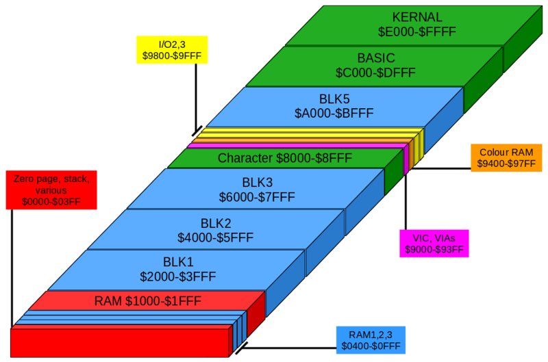
The VIC-20's 6502 Microprocessor can directly address 64KB of memory.
A stock VIC-20 has 5K RAM, and 20K ROM built-in. Furthermore 4K of the address range access I/O devices, including the VIC chip. The I/O area also contains 1K of 4-bit values serving as Color RAM.
A range of 256 bytes, with the base address also divisible by 256 is called a page.
The memory map is divided in 8 blocks, each 8K in length, and numbered 0 to 7.
1 KB low Memory RAM (built-in) in Block 0
- $0000-$00FF: Zeropage
- $0100-$01FF: CPU Stack
- $0200-$03FF: KERNAL and BASIC working areas
3 KB open area in Block 0
- $0400-$07FF: 1 KB, accessed by RAM1 line
- $0800-$0BFF: 1 KB, accessed by RAM2 line
- $0C00-$0FFF: 1 KB, accessed by RAM3 line
4 KB Main RAM (built-in) in Block 0
- $1000-$1FFF: 4 KB, Main RAM
8 KB Expansion Blocks in Blocks 1..3
- $2000-$3FFF: 8 KB, Expansion Block 1, accessed by BLK1 line
- $4000-$5FFF: 8 KB, Expansion Block 2, accessed by BLK2 line
- $6000-$7FFF: 8 KB, Expansion Block 3, accessed by BLK3 line
4 KB ROM, and 4 KB I/O Chip Areas in Block 4
- $8000-$8FFF: 4 KB, Character ROMs, 1k each for glpyhs, lowercase, inverse glyphs, and inverse lowercase
- $9000-$900F: VIC Registers
- $9110-$911F: VIA #1 Registers
- $9120-$912F: VIA #2 Registers
- $9130-$93FF: Unused[A]
- $9400-$97FF: Color RAM (1K of 4 bit nibbles)[B]
- $9800-$9BFF: 1 KB, I/O Expansion 2, accessed by I/O2 line
- $9C00-$9FFF: 1 KB, I/O Expansion 3, accessed by I/O3 line
8 KB Expansion Area in Block 5
- $A000-$BFFF: 8 KB, Expansion Block 5, accessed by BLK5 line. Often used for ROM cartridges. Allows autostart sequence.
16 KB ROM Areas in Blocks 6, and 7
- $C000-$DFFF: 8 KB, Block 6, BASIC Interpreter ROM
- $E000-$FFFF: 8 KB, Block 7, KERNAL ROM
Screen memory map
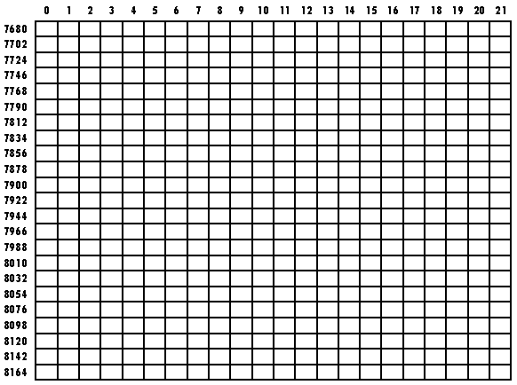
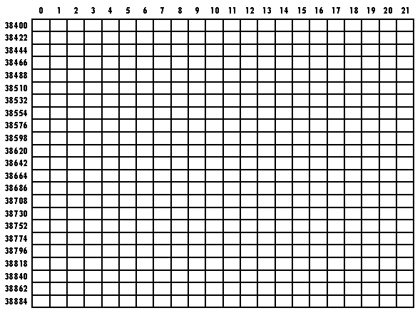
Following is the memory map for the default screen on an unexpanded Vic 20:
Screen Character Codes
Screen Colour Codes
Notes
| A. | This memory range actually repeats the memory windows of the VIC and VIA chips. This is due to the VIC-20's physical design. The entire 1k region of $9000-$9400 sits on a chip select line, but when this line is active, only address lines A0-A3 are connected to the chips, and lines A4-A5 are decoded to select from the three chips. Ergo, $9130-$913F map to nothing (decoder output is unused), $9140-$914F maps to the VIC, $9150-$195F to VIA #1, etc. |
| B. | Color is mapped to $9400-95FF or $9600-$97FF depending upon a setting in the VIC registers. Typically, it is $9600-$97FF on an unexpanded or 3k expanded VIC, otherwise it is at $9400-95FF. |


